Download
1 / 6
70 likes | 317 Views
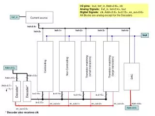
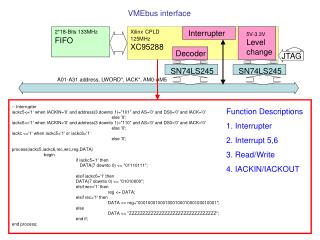
VMEbus interface. 2*18-Bits 133MHz FIFO. Xilinx CPLD 125MHz XC95288. Interrupter. 5V-3.3V Level change. Decoder. JTAG. SN74LS245. SN74LS245. A01-A31 address, LWORD*, IACK*, AM0-AM5. -- Interrupter

E N D
VMEbus interface 2*18-Bits 133MHz FIFO XilinxCPLD 125MHz XC95288 Interrupter 5V-3.3V Level change Decoder JTAG SN74LS245 SN74LS245 A01-A31 address, LWORD*, IACK*, AM0-AM5 -- Interrupter iackc5<='1' when IACKIN='0' and address(3 downto 1)="101" and AS='0' and DS0='0' and IACK='0' else '0'; iackc6<='1' when IACKIN='0' and address(3 downto 1)="110" and AS='0' and DS0='0' and IACK='0' else '0'; iackc <='1' when iackc5='1' or iackc6='1' else '0'; process(iackc5,iackc6,rec,wrc,reg,DATA) begin if iackc5='1' then DATA(7 downto 0) <= "01110111"; elsif iackc6='1' then DATA(7 downto 0) <= "01010000"; elsif wrc='1' then reg <= DATA; elsif rec='1' then DATA <= reg+"00010001000100010001000100010001"; else DATA <= "ZZZZZZZZZZZZZZZZZZZZZZZZZZZZZZZZ"; end if; end process; Function Descriptions 1. Interrupter 2. Interrupt 5,6 3. Read/Write 4. IACKIN/IACKOUT
VMEbus interface 2*18-Bits 133MHz FIFO XilinxCPLD 125MHz XC95288 Interrupter 5V-3.3V Level change Decoder JTAG SN74LS245 SN74LS245 A01-A31 address, LWORD*, IACK*, AM0-AM5 **************************** Resource Summary **************************** Macrocells Product Terms Registers Pins Function Block Used Used Used Used Inputs Used 218/288 ( 75%) 934 /1440 ( 64%) 91 /288 ( 31%) 81 /168 ( 48%) 644/864 ( 74%) PIN RESOURCES: Signal Type Required Mapped | Pin Type Used Remaining ------------------------------------|--------------------------------------- Input : 28 28 | I/O : 80 80 Output : 20 20 | GCK/IO : 1 2 Bidirectional : 32 32 | GTS/IO : 0 4 GCK : 1 1 | GSR/IO : 0 1 GTS : 0 0 | GSR : 0 0 | ---- ---- Total 81 81 Adopt from vmebus.rpt
VMEbus interface 2*18-Bits 133MHz FIFO XilinxCPLD 125MHz XC95288 Interrupter 5V-3.3V Level change Decoder JTAG SN74LS245 SN74LS245 A01-A31 address, LWORD*, IACK*, AM0-AM5 Adopt from sn74v245.pdf
Capture and record 1GHz signal (Realized circuit) Xilinx Spartan-3 XC3S400 500MHz synchronous latch 250MHz synchronous clock XC18V02 National Semiconductor ADC081000 4 ports 8-bits 250MHz MUX 4 ports 8-bits 250MHz FIFO 4 ports 8-bits 250MHz Level 1 Cut Comparator 4 ports 8-bits 250MHz Level 2 Cut Comparator 1GHz Analog Signal 2 ports 8-Bits 500MHz LVDS Data JTAG 1GHz Clock signal 250MHz synchronous clock 8 ports 16-bits 125MHz Encoder Time Counter Trigger 4*32-Bits 125MHz Dual-port RAM 70T3519 XC18V01 XilinxCPLD 125MHz XC95288 Interrupter 5V-3.3V Level change Decoder JTAG SN74LS245 SN74LS245 A01-A31 address, LWORD*, IACK*, AM0-AM5
Xilinx CPLD XC95288 AD FADC ADC081000 Xilinx Spartan-2 XC2S100 Xilinx Spartan-3 XC3S400