Download
1 / 19
200 likes | 489 Views
Overall Project Objective: Design a high speed Viterbi Decoder. Stage 10: 5 th April. 2004 Final Design Corrections. Viterbi Decoder: Presentation #10. Omar Ahmad Prateek Goenka Saim Qidwai Lingyan Sun. M1. Design Manager: Yaping Zhan. Status. Design Proposal: (Done)

E N D
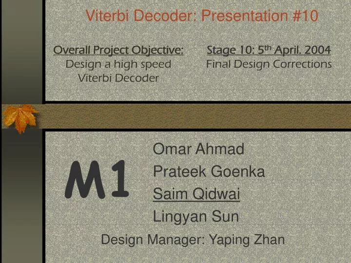
Overall Project Objective: Design a high speed Viterbi Decoder Stage 10: 5th April. 2004 Final Design Corrections Viterbi Decoder: Presentation #10 Omar Ahmad Prateek Goenka Saim Qidwai Lingyan Sun M1 Design Manager: Yaping Zhan
Status • Design Proposal: (Done) • Architecture Proposal: (Done) • Gate level Design: (Done) • Component Layout (DRC & LVS): (Done) • Component Simulation: (Done) • Chip Layout: (Done) • Critical Path Simulation (Done) 18-525, Integrated Circuits Design Project
clk Viterbi Decoder rst Out_valid In_valid Out_data In_data Schematic: top level 18-525, Integrated Circuits Design Project
Layout – Entire Chip 18-525, Integrated Circuits Design Project
Tolerance (Matlab Simulation Result) 18-525, Integrated Circuits Design Project
Critical Path Extraction I + + DFF DFF MUX COMP + + + 18-525, Integrated Circuits Design Project
Critical Path Extraction II 18-525, Integrated Circuits Design Project
Input Pattern Selection Worst case pattern for adder: 011001 and 001001 Worst Case pattern for Comp: two Inputs are the same: 011001 vs. 011001 100111 + 011001 000000 Decision : Use input pattern 011001 and 001001 for both adders DFF MUX COMP + + 18-525, Integrated Circuits Design Project
Simulation Results (500 Mhz.) Note: Time values are in ps. 18-525, Integrated Circuits Design Project
Critical Path I Testing Speed: 500 MHz 18-525, Integrated Circuits Design Project
Critical Path I: Propagation Delay I Propagation Delay: 365ps 18-525, Integrated Circuits Design Project
Critical Path I: Rise Time Rise Time: 619 ps 18-525, Integrated Circuits Design Project
Critical Path I: Fall Time Fall Time: 327 ps. 18-525, Integrated Circuits Design Project
Critical Path II Testing Speed: 500 MHz 18-525, Integrated Circuits Design Project
Critical Path II: Propagation Delay I Propagation Delay: 390 ps. 18-525, Integrated Circuits Design Project
Critical Path II: Rise Time Rise Time: 717 ps. 18-525, Integrated Circuits Design Project
Critical Path II: Fall Time Rising Time: 376 ps. 18-525, Integrated Circuits Design Project
Summary Total Area: 309.96 um x 231.48 um = 71,749.54 sq. um Transistor Count: 17,857 Transistor Density: 0.249 Aspect Ratio: 1.339 Estimated Clock Speed: 300 MHz. Clock Speed Achieved: 500 MHz. 18-525, Integrated Circuits Design Project
Questions 18-525, Integrated Circuits Design Project