Download
1 / 38
380 likes | 542 Views
ECE 448: Spring 11 Lab 3 Sequential Logic for Synthesis. Agenda for today. Introduction: Why are we here? Part 1: Pseudorandom Random Number Generators Part 2: Debouncing Circuit Part 3: Rising Edge Detector Part 4: Counter Part 5: Clock Divider Part 6: Basys II

E N D
ECE 448: Spring 11 Lab 3 Sequential Logic for Synthesis
Agenda for today Introduction: Why are we here? Part 1: Pseudorandom Random Number Generators Part 2: Debouncing Circuit Part 3: Rising Edge Detector Part 4: Counter Part 5: Clock Divider Part 6: Basys II Part 7: FPGA Design Flow based on Aldec Active-HDL
Introduction • Purpose- Test basic circuits on the Basys II • Counter • Debouncing circuit • Rising edge detector • Introduction to Pseudo-Random Number Generator (PRNG) • Introduction to FPGA Design Flow based onAldec Active-HDL
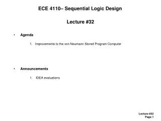
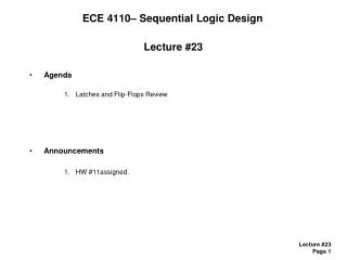
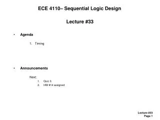
Debouncer test Generic n=8 Counter Generic n=8 Counter 7-Seg Display Unit clk_1k sw(3:0) zeros(7:4) 15:8 7:0 8 rst_i 8 rst_i 8 button(2) button(2) data_o data_o step_i step_i en_i en_i DEBOUNCER RED RED button(0) button(1) clk_i clk_i clk_50M Notation: RED – Rising Edge Detector
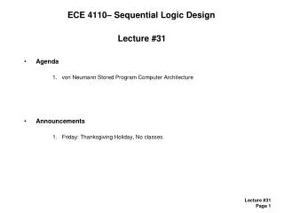
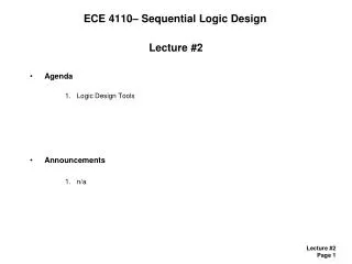
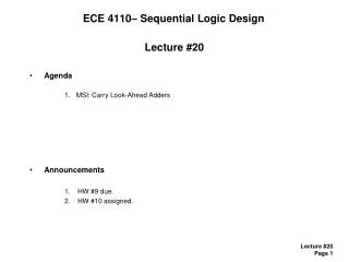
Top-level Circuit for Lab 3 rst_i 8 PRNG 7-Seg Display Unit clk_1k data_o 15:8 7:0 Generic n=8 Counter en_i 8 rst_i button(2) button(2) data_o en_i DEBOUNCER RED button(0) clk_i clk_i clk_50M Notation: RED – Rising Edge Detector
Part 1 Pseudo-Random Number Generator
PRNG • Also known as Deterministic Random Bit Generator (DRBG) • Generates a sequence of numbers that approximates the properties of random numbers. • The sequence is fully deterministic, i.e., it can be repeated based on an initial state of PRNG. • The period of the sequence may be made very large (typically, 2n-1, where n is an internal state size)
PRNG • Random Numbers are often important • Testing of VLSI circuits • Cryptography • Monte Carlo simulations • Noise addition • Bit error detection, and many other applications
Three Initialization Options Option 1 (required): Initialization to ALL ONES, using the signal SET common to all shift registers (connected to rst_i). Option 2 (required): Initialization to ALL ONES by shifting '1’ to all shift registers for 6 clock cycles after reset. Option 3: (bonus): Initialization to arbitrary value, by shifting in internal state serially, using special input sin, one bit per clock cycle.
PRNG Test Vectors Clock Cycle Output 11 D9 12 31 13 87 14 38 15 95 16 19 17 5c 18 CE 19 7E 20 52 Clock Cycle Output 1 FF 2 74 3 BD 4 67 5 EA 6 AE 7 4E 8 5B 9 6A 10 62
Part 2 Debouncing Circuit
Debouncer Capacitance in the button and contacts “bouncing” causes spurs that cause false positives. A debouncing circuit removes these spurs.
Debouncer When the first change is detected, we ignore all subsequent changes for some period of time, preferably until all of the bouncing would have occurred. This is usually on the order of ms.
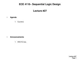
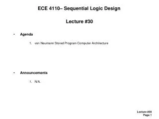
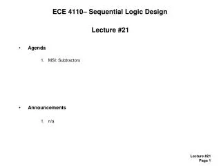
Debouncer Debouncer reset output input clk
Part 3 Rising Edge Detector
Rising Edge Detector • Turn a step function into an impulse • Allows a step to run a circuit for only one clock cycle • Can also be used to cross clock domains Rising Edge Detector
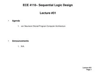
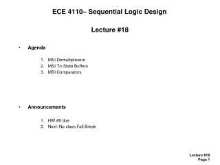
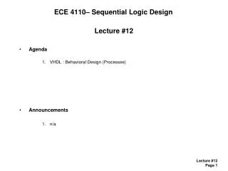
Rising Edge Detector rising edge detector data_i data_o clk_i clk_i data_i data_o
Part 4 Counter
Counter • Count whenever enable signal is high • Synchronous reset • Data out is valid after one clock cycle • Increment step size is configurable • Why use a generic? • Generics make circuits reusable
Counter Generic n Counter n rst_i data_o n step_i en_i clk_i
Counter n Register step_i rst_i n n data_o 0 1 n en_i clk_i
Part 5 Clock Divider
Clock Divider 1 rst_i en_i Counter n = c n data_o en step_i clk_o clk_i
Part 6 Basys II
Basys II Expansion ports VGA connector 7 Segment Displays (4) ON/OFF Switch Buttons (4) Switches (8) LEDs (8)
Basys 2 I/O Circuits
Seven Segment Display • By lighting different combinations of LEDs, different figures appear • For Instance CA, CB, CC make ‘7’ • Common anode means that writing a ‘0’ to CA-DP illuminates the led, where a ‘1’ turns it off
Seven Segment Display • SSRegCtrl has a 16 bit input that is divided into four 4-bit digits • AN(0:3) select which 7 segment display to output to • Digilent recommends a digit period of between 1kHz and 60Hz
Part 7 FPGA Design Flow based on Aldec Active-HDL
FPGA Design process (1) Design and implement a simple unit permitting to speed up encryption with RC5-similar cipher with fixed key set on 8031 microcontroller. Unlike in the experiment 5, this time your unit has to be able to perform an encryption algorithm by itself, executing 32 rounds….. Specification (Lab Assignments) On-paper hardware design (Block diagram & ASM chart) VHDL description (Your Source Files) Library IEEE; use ieee.std_logic_1164.all; use ieee.std_logic_unsigned.all; entity RC5_core is port( clock, reset, encr_decr: in std_logic; data_input: in std_logic_vector(31downto0); data_output: out std_logic_vector(31downto0); out_full: in std_logic; key_input: in std_logic_vector(31downto0); key_read: out std_logic; ); end AES_core; Functional simulation Synthesis Post-synthesis simulation
FPGA Design process (2) Implementation Timing simulation Configuration On chip testing