Download
1 / 11
110 likes | 189 Views
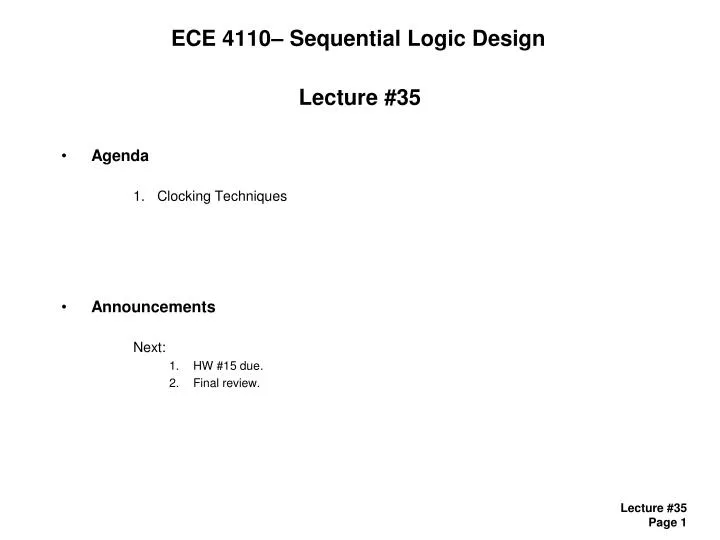
ECE 4110– Sequential Logic Design. Lecture #35 Agenda Clocking Techniques Announcements Next: HW #15 due. Final review. D. D. Q. Q. Clocking Techniques.

E N D
ECE 4110– Sequential Logic Design Lecture #35 • Agenda • Clocking Techniques • Announcements Next: • HW #15 due. • Final review.
D D Q Q Clocking Techniques • Synchronous Clocking- when the same clock is distributed to each flip-flop, there is the chance of clock skew- this clock skew has to be considered as uncertainty when calculating the maximum clock frequency- data lines can also have skew. This is especially an issue when designing a bus
D D D Q Q Q 90 deg Clocking Techniques • Source Synchronous Clocking- to reduce the clock/data skew, a local clock can be generated and sent along with a subset of bus data. - the advantage of creating the clock and data in the same spatial region is: 1) Less geography to cover 2) Less change in material properties 3) Tighter timing can be achieved between clock and data within that group- a bus is divided into groups and a clock is created for each group- the Rx latches that bus group using its associated "source synchronous"- the clock is also commonly called a "Strobe"
Clocking Techniques • Dual Data Rate (DDR)- if the skew is reduced enough, then we can use both edges of the clock to latch data- this doubles the effective data transfer without changing the frequency of the clock- this technique can be used to "Double" the bus frequency or to reduce the number of lines/pins on the bus- the Rx has a Demux/Latch circuit to produce two separate data signals synchronized to one edge of clock so that the information can be used by the internal circuitry on the Rx.
Clocking Techniques • Parallel vs. Serial- the move from parallel to serial buses means trying to send the same (or more) data using less physical lines/pins in the system- other factors besides cost that drive this movement: 1) Area - less pins reduces cost - less pins reduces the size of the overall package - smaller package means - less material, less assembly, more parts per wafer (yield) 2) Simultaneous Switching Noise (SSN) - when signals share a VDD or GND pin, the amount of current through that pin grows as the number of sharing signal pins grows - pins tend to be inductive and cause a L(di/dt) voltage when current is pulled through - there is also Inductive and Capacitive coupling between signal pins causing noise
Clocking Techniques • Differential Signaling - we can use two lines to send one piece of information- one side sends the original signal (A or P) and the other sends the complementary (B or N)- a diff amp style receiver is used to perform A-B (or P-N) to obtain the original signal
Clocking Techniques • Differential Signaling - Disadvantages 1) Takes two pins- Advantages 1) pins provide their own return path 2) the received voltage is doubled (P-N) and always centered at 0v 3) coupling between signal pins is consistent and predictable
Clocking Techniques • Differential Signaling - Advantages 4) noise present on both A and B is removed - this is called "Common Mode Rejection"
D D Q Q ClockData Recovery Clocking Techniques • Embedded Clocking- the only way to get rid of clock/data skew is to get rid of the clock- in Embedded Clocking, the data is encoded such that a certain number of transitions are guaranteed- this gives a consistent and known spectrum- a low speed reference clock is fed to the Rx.- a Phase Locked Loop (PLL) is used to compare the incoming encoded data stream and Ref Clock- the PLL can create a perfectly synchronized clock at the same frequency as the incoming data
Clocking Techniques • Embedded Clocking- this technique completely removes clock/data skew since the phase (i.e., timing relationship) comes from the data itself- to address SSN, Differential Signaling is used- to address DC Drift, an AC coupling capacitor is used on the line. - the AC coupling capacitor passes AC and blocks DC - since the encoded signal is always toggling (due to encoding), the signal passes through the capacitor (i.e., it is AC coupled) - the DC offset of the signal can now be inserted by the receiver wherever it wants - it is typically centered at the "sweet spot" of the Rx's DC input range
Clocking Techniques • Clocking SummaryTechnology SpeedsDetailsApplicationSynchronous up to 400Mb/s SE Data/Clock PCI Bus, uControllersSource Synchronous up to 1600 Mb/s SE Data, Diff Clock DDR, P4 Embedded Clock up to 3.125Gb/s + Diff Signaling PCI Express, SATA, future AC Coup