Download
1 / 22
220 likes | 386 Views
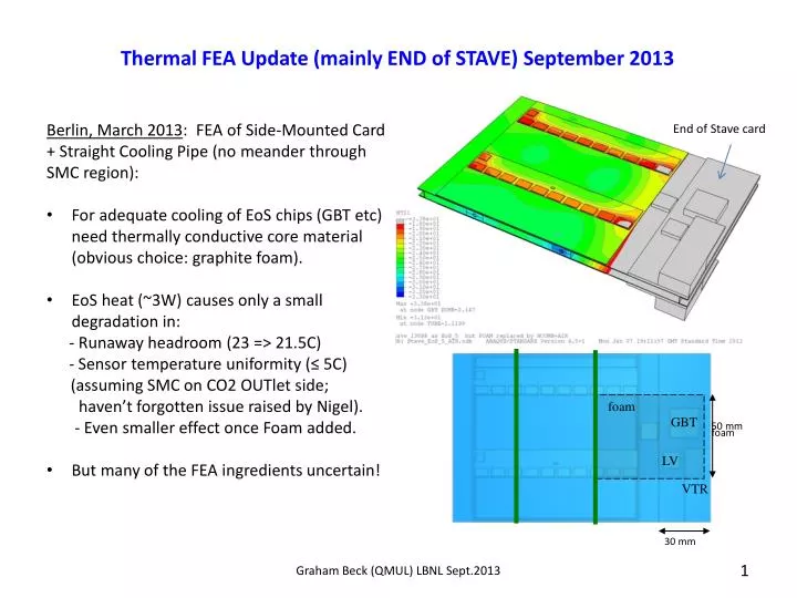
foam. GBT. 50 mm foam. LV. VTR. 30 mm. Thermal FEA Update (mainly END of STAVE) September 2013. Berlin, March 2013 : FEA of Side-Mounted Card + Straight Cooling Pipe (no meander through SMC region):

E N D
foam GBT 50 mm foam LV VTR 30 mm Thermal FEA Update (mainly END of STAVE) September 2013 • Berlin, March 2013: FEA of Side-Mounted Card + Straight Cooling Pipe (no meander through SMC region): • For adequate cooling of EoS chips (GBT etc) need thermally conductive core material (obvious choice: graphite foam). • EoS heat (~3W) causes only a small degradation in: • - Runaway headroom (23 => 21.5C) • Sensor temperature uniformity (≤ 5C) • (assuming SMC on CO2 OUTlet side; • haven’t forgotten issue raised by Nigel). • - Even smaller effect once Foam added. • But many of the FEA ingredients uncertain! End of Stave card Graham Beck (QMUL) LBNL Sept.2013
17x17 mm2 PCB: Assume 2x17mm Cu planes (! heat spreading near chip). Thermal Vias: Not in FEA (needs design): could reduce DT by ×3? 0.5mm Copper spreader (top) 0.7/0.3mm x 5 x 5mm2 chip 3mmPlastic Substrate 20x20 BGA ~0.4mm. ~ 8 layer PCB: 1.6mm FR4 • (Some) Factors that affect GBT die temperature: • GBT Power (estimate:1.8W, more recently: 2.2W “flat out”) • GBT Package resistance - unknown at Berlin meeting (assumed 10 C/W). • Thermal resistance of PCB (especially vias) • Foam (+ CFRP) conductivity and distance between GBT and pipe. • FEA prediction (Berlin): • +11C (operation, CO2 at -30C) / +56C (commissioning, above dew-point)… • GBT Package: • High terminal count => 20x20x0.8mm pitch Plastic Ball Grid Array package. • Procurement chain: CERN – IMEC – ASE (Adv. Semi. Engineering, Taiwan) <= communications slow! • IMEC advised die thermal resistance to ambient probably high (~ 30 C/W) => package with Copper heat spreader and remove heat from TOP. • As of Berlin mtg: May 2013: Packaged die at CERN. Power→Ground shorted (most functions test-able after some surgery). Paulo Moreira stressed package NOT optimised for heat removal via BGA (I guess: vias, trace thickness..) One sample obtained by QMUL to investigate thermal resistance to BOTTOM of package. Graham Beck (QMUL) LBNL Sept.2013
Note thin (0.25mm) die. Capacitors, but no clock or Copper heat slug. 0.54 0.34 ~ 5.4 1.14 0.5 dia / 0.8 pitch 17 Dims (mm) measured at QMUL Thermal Resistance die-to-bottom measured in “TIMTower”: Graham Beck (QMUL) LBNL Sept.2013
Two vertical copper bars sandwiching GBT (+ RS grease); chilled plate stabilises lower T; • Heat injected into upper bar: 2-3W (inferred from dT/dx). Typical contact force (load cell) ~ 10-20N. • Bottom photo: larger Cu block to sink heat from full BGA area. • IR profile => ~ 10C discontinuity between upper and lower bars. ~15% (total) correction for grease at die and BGA (biggest uncertainty) gives package DT. • 6.5 (±1.5) C/W through-packageresistance. • Suggests heat removal through BOTTOM of package alone is adequate. • FEA comparison between this set-up and pcb-mounted package would be instructive. • GBT mounted on a prototype pcb sample (DESY?) would be very useful. Graham Beck (QMUL) LBNL Sept.2013
Not to Scale ! GBT PCB FOAM Appreciable thermal Resistances through GBT Package, PCB and Foam. Use of graphite foam in EoS region (as thermal and mechanical core) seems sensible, but if GBT is located far from pipe may need foam K > 30W/mK. (Need progress on PCB layout) Would like to understand the limitations on available K and dimensions (thickness, area) ! Cooling geometry may also be restricted by other structures at the stave end (next slides). Graham Beck (QMUL) LBNL Sept.2013
Next: • Slides from Peter Sutcliffe, UK engineering meeting (Oxford, 5th Sept.) • (+ my annotations) • CAD drawing of End of Stave • Electrical Break in Pipes (Richard French investigating these): We are looking at the possibility to embed them in Stave core to avoid stress … Graham Beck (QMUL) LBNL Sept.2013
EoS Area • SMC card incorporated the general idea of flex sandwiched between 2 FR4 pcb’s. • SMC Size 98 x 30 • Interlink isn't right.... • Opto height and chips correct to latest models. (GAB) Note the 100 x 50 mm2 SMC area: conservatively large? - implies a long cooling path for GBT, VTR. Top – bottom flex.
ELECTRICAL BREAKS: Ti-Alumina-Ti. Idea to embed in end of stave, to support / avoid stressing them: View of Electrical break in the stave This arrangement reduces pipe length that cools module and SMC by about 20mm – will explore with FEA. New Closeout 0.2mm Radial Gap to Inner CF Skin Wrap with Kapton Tape to insulate
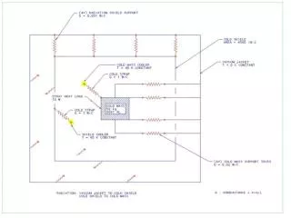
Cooling Path & Headroom away from ends of Stave No Sensor heat SP case 1C bands Relative Thermal Path resistance in cylindrical region, close to 2mm dia pipe: Thickness L(mm) K(W/mK) L/K (~R) Foam (at small R) ~1 30 0.03 Joint:Hysol+BN 0.1 1.6 0.06 Ti pipe 0.14 16.4 0.01 Fluid Film equiv. 0.1 0.8 0.13 (@ 8000W/m2K) -30C -33C • Most important contribution to thermal R in pipe region is the fluid film. • Foam – pipe glue joint assembly needs care, to avoid poor joint / thermal bottleneck. • 30W/mK Foam is fine here! (+ good coupling geometry) • (Path across stave surface is as important: sensor // facing, through bus tape & glue…) • FEA (2011): Runaway Headroom for -30C coolant is 21.5o (23o if allow for P drop). • MUST update FEA: power, conductivities, CFRP density, hybrid layout, on-sensor DCDC…(in progress: don’t anticipate more than 2C change). • Very safe headroom - largely due to locating cooling pipes in core: distributes cooling across module*AND* naturally uses full pipe length for cooling. (If omit foam around the U-bend, lose ~30% runaway headroom). (v. backup slide for comparison with CMS.) Graham Beck (QMUL) LBNL Sept.2013
ACTIONS GBT Package: Do we alert CERN (Paulo Moreira) that we want to cool GBT through its base: omit Copper slug and maybe enhance package conductance? (Maybe wait for pcb trial?) Understand VTR cooling requirement: maybe not critical (some leads from Todd Huffman). Push DESY on PCB dimensions and vias Thermal FEA Update => Establish conductivity of Foam required to cool GBT etc. + … Acceptable chip temperatures depend on our understanding reliability issues Graham Beck (QMUL) LBNL Sept.2013
BACKUP Graham Beck (QMUL) LBNL Sept.2013
Thicker stave to Accommodate New, slightly smaller, Electrical Break Old Break ELECTRICAL BREAKS: Dimensions here are indicative and driven by need to try out the concept! New break: Larger exit tube Slightly smaller OD of 4.8
COMMENT re Module Cooling geometry. CMS Upgrade Strip modules (Andreas Mussgiller, Oxford Tracker Forum, June 2013) • CO2: -34C • Module cooling contacts -27C • (Sensor Tmax ~ -20C) • (At 3000 fb-1): Runaway when module cooling contacts reach -25C • runaway headroom is2 degrees • (trying to improve on this). Graham Beck (QMUL) LBNL Sept.2013
Plots from Steve McMahon of Current SCT temperature: Graham Beck (QMUL) LBNL Sept.2013
NEAR End of Stave (but away from SMC): Temperature variation across Sensor. No Sensor heat SP case 1C bands dcdc -30C Fluid -33C • No sensor heat (3000 fb-1,-25C expect ~ 0.4W) • Hybrid heat 5.6W/module face (~1mW/chan). • Sensor T Variation due to: • - Hybrid/HCC/Pipe: 3.5C • - Asymmetric fluid T: 2C • gives for: • - SP: ~ 5.5 degrees over sensor area. • - DCDC(edge-mounted): • ~ 4 deg. (fluid as shown) Preferred? • ~ 7 deg. (flow reversed) Uncomfortable? This perhaps sets the scale for acceptable level of T variation due to presence of SMC. Note: The above FEA plot neglects heat flow between modules due to asymmetric hybrid placement. Hybrid placement affects the range of T variation across the sensor: IF symmetrically placed hybrids have become the baseline it would be an advantage to change the model to reflect that! Graham Beck (QMUL) LBNL Sept.2013
FEA Model 30 mm GBT VTR LV (DCDC) -32C -33C -31.5C -30C -31C Conduction to adjacent module is ~ 20%: neglected here. LV and VTR are cosmetic only, apart from heat injected into PCB footprint! GBT is modelled, to have some estimate of die temperature. DESY meeting: wider PCB (50mm?) (For convenience have suppressed honeycomb volumes: were modelled as air) • CO2 Temperature (Boundary Conditions) – refinement of previous FEA! • Pressure drop => Temperature drop of ~ 3C along pipe (will be measured at CERN). • Mean fluid T is 1.5 degrees below input T. (=> correction to Runaway Headroom: now “23C wrt input fluid”) • Fluid T vs Z: ~ equal at Z=0, increasingly asymmetric towards EoS. • In presence of other sources of asymmetry, direction of flow matters! Graham Beck (QMUL) LBNL Sept.2013
Convection +Radiation - appreciable since the SMC and chips are at relatively high T.- included crudely in the model as a surface film effect at the pcb surface (biggest contribution):htc 10 W/m2K ; ambient T -23.5C (approx. mean stave surface T).- accounts for about 0.4W (15% ) heat loss from the SMC. - lowers the GBT chip T by typically 5C.Where does the heat go? At worst, it is a 0.5W load on the module below ( <10% hybrid heat ) - Ignored in the FEA. Graham Beck (QMUL) LBNL Sept.2013
Additional Strategy: Divert the Cooling Pipe towards the SMC – Somehow shape pipe (e.g. zig-zag to reduce distance to SMC? Tricky. . . e.g. Shift pipe 20mm towards SMC => Further cools GBT by 3C. BUT: Knocks 4C off Runaway Headroom!WHY?- STAVE Cooling philosophy is to distribute the cooling pipes evenly across the sensor. . .Disturbing this increases thermal resistance RT (Sensor Heat => Coolant) (above: by 16%).(A change in R that increases the sensor T (in absence of leakage current) by DT reduces the headroom by ~ 3xDT. Changing R is 3x as dangerous as changing Q, cf straight pipe result).- Introducing a small meander into the pipe to help cool the SMC (or for other reasons) can seriously harm the runaway headroom: could be done but would involve some TLC and yet more foam …. Material Cost of Foam: Foam 56 x 98 x 4mm total, r = 0.25, X0 = 43g/cm2: 0.13 cm2 cfTi pipe wiggle: 36cm x 2mm id x 0.14mm wall, r = 4.51, X0 = 16.2 g/cm20.1 cm2 SMC boards - !!FR4 ONLY 3 x 10 x 0.16 cm3, X0 = 16.8cm : 0.6 cm2 - conclude no need to worry about foam inserts (use more if helps?). 20 Graham Beck (QMUL) LBNL Sept.2013
17x17 mm2 PCB: Assume 2x17mm Cu planes (! heat spreading near chip). Thermal Vias: Not in FEA (needs design): could reduce DT by ×3? 0.5mm Copper spreader (top) 0.7/0.3mm x 5 x 5mm2 chip 3mm Plastic Substrate 20x20 BGA ~0.4mm. ~ 8 layer PCB: 1.6mm FR4 EoS COMPONENTS - THERMAL VTR: Assumephysically similar to SMU design (Dual Tx for Calo): Transmitter: 217mW (LpGBLD 40% lower. Still in 130nm) Receiver: 120mW (+ PIN diode ff. Rad.damage ?) (? Jan Troska, AUW: “VTR doesn’t need active cooling”) FEA: VTR NOT modelled thermally (only cosmetic)…. Inject VTR Heat into connector footprint. GBT: 1.8W (Lp version - 65nm Schedule+Reliability issues.) Package: ASE(Taiwan) via IMEC: Not final package? Thermal R (die => board) not known (aim to measure!). FEA: Assume 10C/W (experience with Motorola MCP7447A ceramic). Model as isotropic, K = 1.4W/m-K. Power Conversion: Useful Power 2.14W Assume (aggressive) 75% efficiency => 0.7 W (conversion) Total SMC power (per face)2.84W (equiv.to ~ ½ hybrid power) Graham Beck (QMUL) LBNL Sept.2013