Download
1 / 27
270 likes | 282 Views
8.0 Operational Amplifier 8.1 Op-Amp Operation 8.2 Op-amp Input Mode and Parameters 8.3 Op-Amp Basic 8.4 Closed-loop Op-amp 8.5 Op-amp Compensation 8.6 Frequency Response 8.7 Op-Amp Application. Operational Amplifier.

E N D
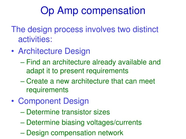
8.0 Operational Amplifier 8.1 Op-Amp Operation 8.2 Op-amp Input Mode and Parameters 8.3 Op-Amp Basic 8.4 Closed-loop Op-amp 8.5 Op-amp Compensation 8.6 Frequency Response 8.7 Op-Amp Application
Operational Amplifier • Many transistors, diodes, resistors, capacitors are fabricated on a single tiny chip of semiconductives material and packaged in a single case to form functional circuit – linear integrated circuits (ICs). • Example of ICs is operational amplifier (op-amps). • Op-amps were used primarily to perform mathematical operations such as +, -, integration, differentiation and work with high voltage. • Now op-amps use low dc power voltages and inexpensive.
1 8 Inverting input - Output NC Invert V+ Noninvert Output + V- Noninverting input 8.1 Op-Amp Operation Ideal Op-amps has infinite voltage gain and infinite bandwidth. Also it has infinite input impedance and zero output impedance.
The op amp is built using VLSI techniques. Basic Op-Amp typically use 22 transistors and 12 resistors.
Op-Amp Characteristic Ideal op-amp has infinite voltage gain and infinite bandwidth. Also it has infinite input impedance (open) so that it does not load the driving source and it has zero output impedance. Practical op-amp are very high voltage gain, very high input impedance, very low output impedance and wide bandwidth.
Internal Block Diagram of an Op-Amp Typical op-amp made-up of 3 types amplifier circuits ; • input stage (A) – differential amplifier (provides amplification of the difference voltage between 2 inputs) • gain stage (B) - voltage amplifier (usually class A amplifier which provides additional gain) • output stage (C) - class B push-pull amp - A Vout B C Vin + Basic internal arrangement of an op-amp
The differential amplifier was introduced in BJT amplifier chapter. • The term differential comes from the mplifier’s ability to amplify the difference of 2 input signals applied to its inputs. Only the difference in the 2 signals is amplified; if there is no difference, the output is zero. • The differential amplifier exhibits 2 modes of operations ; differential mode and common mode.
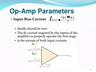
8.2 Op-amp Input Mode and Parameters In single ended input mode one input is grounded and signal voltage is applied only to other input. In differential input mode 2 out-of-phase signals are applied with the difference of 2 amplified and produced at the output. In common mode input, 2 signals of same phase, frequency, and amplitude are applied to the inputs, they cancel each other, which results in no output. This is called common-mode rejection. This type of mode is used for removal of unwanted noise signals.
Common-mode rejection ratio (CMRR) is the measure for how well it rejects an unwanted signal. It is the ratio of open loop gain, Aol to common-mode gain, ACM. The higher CMRR the better (means open loop gain is high and common mode gain is low) CMRR = Aol /Acmor 20log(Aol/Acm) dB Aol of an op-amp is the internal voltage gain of the device and represents the ratio of the output voltage to input voltage when there are no external components. Input offset voltage, VOS is difference in voltage between inputs that is necessary to make Vout(error) = 0 (ideal for 0 and normally less than 2 mV).
Electrical Characteristic Note these ratings are for specific circuit conditions, and they often include minimum, maximum and typical values.
Op-Amp Gain Open-loop refers to where there is no feedback from output back to the input. In open-loop gain can exceed 100,000 so only small input can drive it into saturation. Closed-loop reduces the gain. In order to control the gain of an op-amp it must have feedback. This feedback is a negative feedback. Av negative feedback will reduce the gain and improve many characteristics of op-amp. Input is applied to inverting (-) input, non-inverting input (+) is grounded. Resistor Rf is feedback resistor. This is negative feedback, where 1800 phase shift between input and output.
8.4 Closed-loop Op-Amp Noninverting Amplifier Closed-loop voltage gain, Acl is voltage gain of an op-amp with external feedback. Gain can be controlled by external component values. Feedback voltage, Vf = (Ri/(Ri + Rf))Vout Vout = (Vin – Vf)Aol Feedback attenuation, B = Ri/(Ri + Rf) So, Vout = Aol(Vin – BVout) Vout(1 + AolB) = AolVin Acl(NI) = Vout/Vin = Aol/(1 +AolB) ≈ 1/B, Since AolB> 1 =(Ri + Rf)/Ri = 1 + (Rf / Ri)
Input Impedance Assume small differential voltage, Vd exist between two input, where it’s input impedance is not infinite and input current is not zero. so Vin = Vd + Vf, but Vf = BVout and B = Ri/(Ri + Rf) Vin = Vd + BVout, where Vout = AolVd Vin = Vd + AolBVd = (1 + AolB)Vd and Vd = IinZin, where Zin is open loop input impedance Vin = (1 + AolB)IinZin so input impedance, Zin(NI) = Vin/Iin = (1 + AolB)Zin So input impedance of noninverting amplifier with negative feedback is higher than without feedback.
Output Impedance KVL : Vout = AolVd – ZoutIout Where Vd = Vin – Vf, and assume AolVd >> ZoutIout So Vout = Aol(Vin – Vf), where Vf = BVout So Vout = Aol(Vin – BVout) AolVin = Vout + AolBVout = (1 + AolB)Vout = (1 + AolB)Zout(NI)Iout Since output impedance, Zout(NI) = Vout/Iout Divide by Iout : (AolVin)/Iout = (1 + AolB)Zout(NI) Without feedback, AolVin = Vout So Zout = Vout/Iout = (1 + AolB)Zout(NI) So Zout is less when with negative feedback.
Therefore zout(NI) = zout/(1+AolB)
Ex : If from data sheet, Zin = 2MΩ, Zout = 75Ω and Aol = 200,000. Find input and output impedance and closed-loop voltage gain. B = Ri/(Ri+Rf) = 10/230 = 0.0435 Zin(NI) = (1+AolB)Zin = 17.4G Ohms Zout(NI= Zout/(1+AolB) = 8.6 m Ohms Acl(NI) = 1 + Rf/Ri = 23
Voltage-Follower Voltage-follower amplifier configuration has all of the output signal fed back to inverting input. Voltage gain Acl(VF)=AV = Vout / Vin = 1 (means is no gain). This makes it useful as a buffer amp since it has a high input impedance and low output impedance
Voltage follower is actually noninverting amp but with B = 1 So Zin(VF) = (1 + Aol)Zin Zout(VF) = Zout/(1 + Aol) Zin(VF) is greater than Zin(NI) but Zout(VF) is smaller than Zout(NI).
Ex: If from data sheet, Zin = 2MΩ, Zout = 75Ω and Aol = 200,000. Find input and output impedance of voltage follower Zin(VF) = (1 + Aol)Zin Zout(VF) = Zout/(1 + Aol) Zin(VF) = 400 G Ohms Zout(VE) = 375 micro Ohms
Inverting Amplifier Inverting amplifier has output fed back to inverting input for gain control. Infinite input impedance implies zero current at inverting input, so no voltage drop between the inputs. Then voltage at inverting input is zero (called virtual ground) because noninverting input is grounded.
Since no current at inverting input, current through Ri and through Rf are equal, Iin = If Voltage across Ri equal Vin coz the resistor is connected to virtual ground at the inverting input, so Iin = Vin/Ri Also the voltage across Rf equal –Vout because of virtual ground, so If = -Vout/Rf Since, If = Iin, -Vout/Rf = Vin/Ri so Vout/Vin, Acl(I) = -Rf/Ri
Input impedance, Zin(I) = Ri, coz inverting input of op-amp is at virtual ground (0V), and input source simply see Ri to ground. Output impedance, Zout(I) = Zout/(1 + AolB) It’s value decrease by negative feedback. Zout for noninverting and inverting is very low, in fact in practical is zero, so that any load impedance connected to op-amp output can vary greatly and not change Vout at all.
EX : If the Acl(I) is -100, find Rf value. Acl(I) = -Rf/Ri -100 = -Rf/2.2 k Ohms Rf = 220 k Ohms
BASIC OP-AMP CIRCUITSSumming Amplifier Because op-amp has a high input impedance the multiple inputs are treated as separate inputs.
Integrators Output is the integral of the input. It is operation of summing the area under a waveform or curve over a period of time. Integrator is easily identified by the capacitor in feedback loop. Constant input voltage yields a ramp output. Slope of ramp is determined by the RC time constant. Integrator can be used to change a square wave input into a triangular wave output. This circuit is useful in low-pass filter circuits and sensor conditioning circuits. Rate of change can be determined by; Vout/Vin = -Vin/RiC
Differentiator Differentiator takes derivative of the input and it’s useful in high-pass filter circuits. Differentiator does opposite of the integrator in that it takes a sloping input and provides an output that is proportional to rate of change of input. Note capacitor is in the input circuit. A triangular input would yield a square wave output. Vout = -(Vc/t)RfC