Download

1 / 36
380 likes | 630 Views
PLDs, FPGAs, and Decoders. Top-down Modular Design. Top-down design is a process in which a function is initially specified at a high level of abstraction and then decomposed into lower-level sub-functions, each of which is more concrete.

E N D
Top-down Modular Design • Top-down design is a process in which a function is initially specified at a high level of abstraction and then decomposed into lower-level sub-functions, each of which is more concrete. • The decomposition process continues until the design is reduced to a set of functions, each of which is well defined and can be realized with a relatively simple circuit. • Hence, the design has been developed from the “top” level “down” to a level at which the individual modules are manageable.
complete the design • After all functions have been defined, each is realized with a circuit module that is designed, implemented, and tested individually. • The finished modules are then interconnected to complete the design. • This implementation process is often referred to as a bottom-up process, since it begins with the bottommost elements of the design and works toward the topmost function.
Programmable Logic Arrays (PLAs) • Any combinational logic function can be realized as a sum of products. • Idea: Build a large AND-OR array with lots of inputs and product terms, and programmable connections. • n inputs • AND gates have 2n inputs -- true and complement of each variable. • m outputs, driven by large OR gates • Each AND gate is programmably connected to each output’s OR gate. • p AND gates (p<<2n)
Programmable Logic Arrays (PLAs) • A PLA is a combinational, two-level AND-OR device that can be programmed to realize any sum-of-products logic expression, subject to the size limitations of the device. • Limitations are: • the number of inputs (n) • AND gates have 2n inputs -- true and complement of each variable. • the number of outputs (m), driven by large OR gates • Each AND gate is programmably connected to each output’s OR gate. • the number of product terms (p AND gates; p<<2n)
Programmable Logic Arrays (PLAs) • Such a PLA is described as n x m PLA with p product terms an n x m PLA with p product terms contains: p 2n-input AND gates and m p-input OR gates. e.g., 4 x 3 PLA with 6 product terms an 4 x 3 PLA with 6 product terms contains: 6 8-input AND gates and 3 6-input OR gates.
Compact representation • Actually, closer to physical layout (“wired logic”).
PLA Electrical Design • A 4 x 3 PLA built using TTL-like open-collector gates and diode logic.
PLA Electrical Design • By applying special input patterns to the device, it is possible to select individual links, apply a high voltage (10-30 v), and thereby vaporize selected links.
PLA Electrical Design • Instead of a diode, an n-channel transistor with a programmable connection is placed at each intersection between an input line and a word line. • Reduced power consumption • reprogrammability
PLA Electrical Design • See Section 5.3.5 -- wired-AND logic
Programmable Array Logic (PALs) • How beneficial is product sharing? • Not enough to justify the extra AND array • PALs ==> fixed OR array • Each AND gate is permanently connected to a certain OR gate. • Example: PAL16L8
10 primary inputs • 8 outputs, with 7 ANDs per output • 1 AND for 3-state enable • 6 outputs available as inputs • more inputs, at expense of outputs • two-pass logic, helper terms • Note inversion on outputs • output is complement of sum-of-products • newer PALs have selectable inversion
EPLDs • An erasable Programmable Logic Device • can be reprogrammed and uses floating-gate MOS transistor.
CPLDs and FPGAs • CPLDs - complex PLDs use floating-gate programming technology. • FPGAs - Field-Programmable Gate Arrays use read/write memory cells to control the state of each connection.
Designing with PALs • Compare number of inputs and outputs of the problem with available resources in the PAL. • Write equations for each output using ABEL. • Compile the ABEL program, determine whether minimimized equations fit in the available AND terms. • If no fit, try modifying equations or providing “helper” terms.
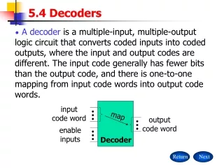
Decoders • A decoder is multiple-input, multiple-output logic circuit that converts coded inputs into coded outputs. • Input code with fewer bits than the output bits. • Typically n inputs, 2n outputs • 2-to-4, 3-to-8, 4-to-16, etc. • There is a one-to-one mapping.
Decoders • General decoder structure • Typically n inputs, 2n outputs • 2-to-4, 3-to-8, 4-to-16, etc.
Binary 2-to-4 decoder Note “x” (don’t care) notation.
MSI 2-to-4 decoder • Input buffering (less load) • NAND gates (faster)
Decoder cascading 4-to-16 decoder
More cascading 5-to-32 decoder
Decoder applications • Microprocessor memory systems • selecting different banks of memory • Microprocessor input/output systems • selecting different devices • Microprocessor instruction decoding • enabling different functional units • Memory chips • enabling different rows of memory depending on address • Lots of other applications
Next time • Encoders • Three-state devices • Multiplexers • XOR gates • Comparators • Adders