Download
1 / 45
580 likes | 846 Views
Lecture 11: Sequential Circuit Design. Outline. Sequencing Sequencing Element Design Max and Min-Delay Clock Skew Time Borrowing Two-Phase Clocking. Sequencing. Combinational logic output depends on current inputs Sequential logic output depends on current and previous inputs

E N D
Outline • Sequencing • Sequencing Element Design • Max and Min-Delay • Clock Skew • Time Borrowing • Two-Phase Clocking 11: Sequential Circuits
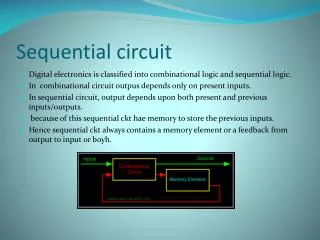
Sequencing • Combinational logic • output depends on current inputs • Sequential logic • output depends on current and previous inputs • Requires separating previous, current, future • Called state or tokens • Ex: FSM, pipeline 11: Sequential Circuits
Latch versus Register • Latch is level sensitive. stores data when clock is low • Flip-Flop (FF) is edge-triggered. stores data when clock rises D Q D Q Clk Clk Clk Clk D D Q Q
Sequencing Elements • Latch: Level sensitive • a.k.a. transparent latch, D latch • Flip-flop: edge triggered • A.k.a. master-slave flip-flop, D flip-flop, D register • Timing Diagrams • Transparent • Opaque • Edge-trigger 11: Sequential Circuits
Sequencing Overhead • Use flip-flops to delay fast tokens so they move through exactly one stage each cycle. • Inevitably adds some delay to the slow tokens • Makes circuit slower than just the logic delay • Called sequencing overhead • Some people call this clocking overhead • But it applies to asynchronous circuits too • Inevitable side effect of maintaining sequence 11: Sequential Circuits
Latch Design • Pass Transistor Latch • Pros + Tiny + Low clock load • Cons • Vt drop • nonrestoring • backdriving • output noise sensitivity • dynamic • diffusion input Used in 1970’s 11: Sequential Circuits
Latch Design • Transmission gate + No Vt drop - Requires inverted clock 11: Sequential Circuits
Latch Design • Inverting buffer + Restoring + No backdriving + Fixes either • Output noise sensitivity • Or diffusion input • Inverted output • Both are fast dynamic latchs 11: Sequential Circuits
Latch Design • Tristate feedback + Static • Backdriving risk • Static latches are now essential because of leakage 11: Sequential Circuits
Latch Design • Buffered input + Fixes diffusion input + Noninverting 11: Sequential Circuits
Latch Design • Buffered output + No backdriving • Widely used in standard cells + Very robust (most important) • Rather large • Rather slow (1.5 – 2 FO4 delays) • High clock loading 11: Sequential Circuits
Latch Design • Datapath latch + smaller + faster • unbuffered input • In semicustom datapath applications where input noise can be better controlled. • Intel uses this as a standard datapath latch. 11: Sequential Circuits
Latch Design • Jamb latch: uses a weak feedback inverter in place of the tristate. + reduces the clock load + saves two transistors requires careful circuit design 11: Sequential Circuits
Latch Design • Jamb latch used in register files and Field Programmable Gate Array (FPGA) cells 11: Sequential Circuits
Latch Design • clocked CMOS (C2MOS) latch • Similar to the conventional latch, but • Conventional latch is faster because the output is driven through parallel nMOS and pMOS. • C2MOS is slightly smaller because it eliminates two contacts. Conventional latch 11: Sequential Circuits
Latch Design 11: Sequential Circuits
Multiplexer-Based Latches 11: Sequential Circuits
Multiplexer-Based Latches • Transistor level • TG based positive latch: • Pass-Tr based • Reduced CLK load Cons: load of 4 transistors to the CLK signal. 11: Sequential Circuits
Flip-Flop Design • most common approach for constructing an edge-triggered register is to use a master-slave configuration. • Is built by combining two level-sensitive latches, one negative-sensitive and one positive-sensitive. 11: Sequential Circuits
Flip-Flop Design inverting dynamic flip-flop With feedback tristates and extra inverter 11: Sequential Circuits
TG-Based FF • Reduced load clock static master-slave FF. • reverse conduction problem • T2 and I4 influence the data stored in I1-I2 latch. 11: Sequential Circuits
Non-ideal clock signals • Clock skew: variation in clock delay to different nodes. Causes clock overlap. • D to Q is open in overlapping time. Thus Q may change on rising edge, which is undesired for a negative edge-triggered FF. • node A can be driven by both D and B, resulting in an undefined state. 11: Sequential Circuits
Non-overlapping Clocks 11: Sequential Circuits
C2MOS Flip-Flop 11: Sequential Circuits
Insensitive to Clock-Overlap V V V V DD DD DD DD M M M M 2 6 2 6 M M 0 0 4 8 X X D Q D Q M M 1 1 3 7 M M M M 1 5 1 5 (a) (0-0) overlap (b) (1-1) overlap 11: Sequential Circuits
TSPC Latches Positive latch (transparent when CLK= 1) Negative latch (transparent when CLK= 0) 11: Sequential Circuits
Including Logic in TSPC Logic inside the latch Example: AND latch 11: Sequential Circuits
Simplified TSPC latch 11: Sequential Circuits
Positive-Edge TSPC Flip-Flop • Clk=0: sampling precharge hold stable • Clk=1: hold evaluate on stable • Homework: negative-edge FF 11: Sequential Circuits
Enable • Enable: ignore clock when en = 0 • Mux • Increase latch D-Q delay • Increase area • Clock Gating • No delay on data input • AND gate can be shared • Reduce power consumption (clock doesn’t toggle) • increase clock delay -> skew 11: Sequential Circuits
Reset • Force output low when reset asserted • Synchronous vs. asynchronous 11: Sequential Circuits
Set / Reset • Set forces output high when enabled • Flip-flop with asynchronous set and reset 11: Sequential Circuits
Sequencing Methods • Flip-flops • 2-Phase Latches • Pulsed Latches 11: Sequential Circuits
Timing Diagrams Contamination and Propagation Delays 11: Sequential Circuits
Max-Delay: Flip-Flops 11: Sequential Circuits
Max Delay: 2-Phase Latches 11: Sequential Circuits
Max Delay: Pulsed Latches 11: Sequential Circuits
Min-Delay: Flip-Flops • If not, delay should be added between the flip-flops (e.g., with a buffer) 11: Sequential Circuits
Min-Delay: 2-Phase Latches Hold time reduced by nonoverlap 11: Sequential Circuits
Min-Delay: Pulsed Latches Hold time increased by pulse width 11: Sequential Circuits
Pipelining Pipelined Reference
Pipelined CMOS 11: Sequential Circuits
Summary • Flip-Flops: • Very easy to use, supported by all tools • 2-Phase Transparent Latches: • Lots of skew tolerance and time borrowing • Pulsed Latches: • Fast, some skew tol & borrow, hold time risk 11: Sequential Circuits