Download
1 / 28
290 likes | 580 Views
Sequential circuit design. Now let’s reverse the process: In sequential circuit design , we turn some description into a working circuit. We first make a state table or diagram to express the computation. Then we can turn that table or diagram into a sequential circuit. Sequence recognizers.

E N D
Sequential circuit design • Now let’s reverse the process: In sequential circuit design, we turn some description into a working circuit. • We first make a state table or diagram to express the computation. • Then we can turn that table or diagram into a sequential circuit. Sequential circuit design
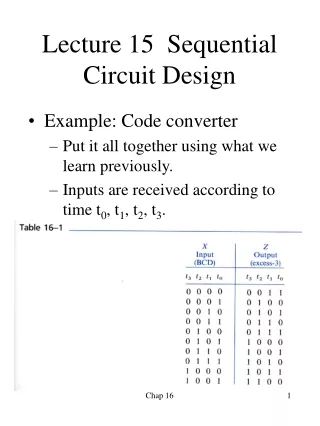
Sequence recognizers • A sequence recognizer is a special kind of sequential circuit that looks for a special bit pattern in some input. • The recognizer circuit has only one input, X. • One bit of input is supplied on every clock cycle. For example, it would take 20 cycles to scan a 20-bit input. • This is an easy way to permit arbitrarily long input sequences. • There is one output, Z, which is 1 when the desired pattern is found. • Our example will detect the bit pattern “1001”: Inputs: 1 1 1 0 0 1 1 0 1 0 0 1 0 0 1 1 0 … Outputs: 0 0 0 0 0 1 0 0 0 0 0 1 0 0 1 0 0 … Here, one input and one output bit appear every clock cycle. • This requires a sequential circuit because the circuit has to “remember” the inputs from previous clock cycles, in order to determine whether or not a match was found. Sequential circuit design
1/0 0/0 0/0 A C D B A basic state diagram • What state do we need for the sequence recognizer? • We have to “remember” inputs from previous clock cycles. • For example, if the previous three inputs were 100 and the current input is 1, then the output should be 1. • In general, we will have to remember occurrences of parts of the desired pattern—in this case, 1, 10, and 100. • We’ll start with a basic state diagram (edges are labeled input/output): Sequential circuit design
Step 1: Making a state table • The first thing you have to figure out is precisely how the use of state will help you solve the given problem. • Make a state table based on the problem statement. The table should show the present states, inputs, next states and outputs. • Sometimes it is easier to first find a state diagram and then convert that to a table. • This is usually the most difficult step. Once you have the state table, the rest of the design procedure is the same for all sequential circuits. • Sequence recognizers are especially hard! They’re the hardest example we’ll see in this class, so if you understand this you’re in good shape. Sequential circuit design
1/0 0/0 0/0 A C D B A basic state diagram • What state do we need for the sequence recognizer? • We have to “remember” inputs from previous clock cycles. • For example, if the previous three inputs were 100 and the current input is 1, then the output should be 1. • In general, we will have to remember occurrences of parts of the desired pattern—in this case, 1, 10, and 100. • We’ll start with a basic state diagram: Sequential circuit design
1/0 0/0 0/0 A C D B 1/1 Overlapping occurrences of the pattern • What happens if we’re in state D (the last three inputs were 100), and the current input is 1? • The output should be a 1, because we’ve found the desired pattern. • But this last 1 could also be the start of another occurrence of the pattern! For example, 1001001 contains two occurrences of 1001. • To detect overlapping occurrences of the pattern, the next state should beB. Sequential circuit design
1/0 0/0 0/0 A C D B 0/0 1/0 1/1 1/0 0/0 Filling in the other arrows • Remember that we need two outgoing arrows for each node, to account for the possibilities of X=0 and X=1. • The remaining arrows we need are shown in blue. They also allow for the correct detection of overlapping occurrences of 1001. Sequential circuit design
0/0 1/0 next state 1/0 input/output 0/0 0/0 A C D present state B 1/0 1/1 0/0 Finally, making the state table Remember how the state diagram arrows correspond to rows of the state table: Sequential circuit design
Sequential circuit design procedure Step 1: Make a state table based on the problem statement. The table should show the present states, inputs, next states and outputs. (It may be easier to find a state diagram first, and then convert that to a table.) Step 2: Assign binary codes to the states in the state table, if you haven’t already. If you have n states, your binary codes will have at least log2 n digits, and your circuit will have at least log2 n flip-flops. Step 3: For each flip-flop and each row of your state table, find the flip-flop input values that are needed to generate the next state from the present state. You can use flip-flop excitation tables here. Step 4: Find simplified equations for the flip-flop inputs and the outputs. Step 5: Build the circuit! Sequential circuit design
Step 2: Assigning binary codes to states • We have four states ABCD, so we need at least two flip-flops Q1Q0. • The easiest thing to do is represent state A with Q1Q0 = 00, B with 01, C with 10, and D with 11. • The state assignment can have a big impact on circuit complexity, but we won’t worry about that too much in this class. Sequential circuit design
Step 3: Finding flip-flop input values • Next we have to figure out how to actually make the flip-flops change from their present state into the desired next state. • This depends on what kind of flip-flops you use! • We’ll use two JKs. For each flip-flip Qi, look at its present and next states, and determine what the inputs Ji and Ki should be in order to make that state change. Sequential circuit design
Finding JK flip-flop input values • For JK flip-flops, this is a little tricky. Recall the characteristic table: • If the present state of a JK flip-flop is 0 and we want the next state to be 1, then we have two choices for the JK inputs: • We can use JK=10, to explicitly set the flip-flop’s next state to 1. • We can also use JK=11, to complement the current state 0. • So to change from 0 to 1, we must set J=1, but K could be either 0 or 1. • Similarly, the other possible state transitions can all be done in two different ways as well. Sequential circuit design
JK excitation table • An excitation table shows what flip-flop inputs are required in order to make a desired state change. • This is the same information that’s given in the characteristic table, but presented “backwards.” Sequential circuit design
Excitation tables for all flip-flops Sequential circuit design
Back to the example • We can now use the JK excitation table on the right to find the correct values for each flip-flop’s inputs, based on its present and next states. Sequential circuit design
Back to the example • We can now use the JK excitation table on the right to find the correct values for each flip-flop’s inputs, based on its present and next states. Sequential circuit design
Step 4: Find equations for the FF inputs and output • Now you can make K-maps and find equations for each of the four flip-flop inputs, as well as for the output Z. • These equations are in terms of the present state and the inputs. • The advantage of using JK flip-flops is that there are many don’t care conditions, which can result in simpler MSP equations. J1 = X’ Q0 K1 = X + Q0 J0 = X + Q1 K0 = X’ Z = Q1Q0X Sequential circuit design
Step 5: Build the circuit • Lastly, we use these simplified equations to build the completed circuit. J1 = X’ Q0 K1 = X + Q0 J0 = X + Q1 K0 = X’ Z = Q1Q0X Sequential circuit design
Step 5: Build the circuit • Lastly, we use these simplified equations to build the completed circuit. J1 = X’ Q0 K1 = X + Q0 J0 = X + Q1 K0 = X’ Z = Q1Q0X Sequential circuit design
1 2 3 4 CLK Q1 Q0 X Z Timing diagram • Here is one example timing diagram for our sequence detector. • The flip-flops Q1Q0 start in the initial state, 00. • On the first three positive clock edges, X is 1, 0, and 0. These inputs cause Q1Q0 to change, so after the third edge Q1Q0 = 11. • Then when X=1, Z becomes 1 also, meaning that 1001 was found. • The output Z does not have to change at positive clock edges. Instead, it may change whenever X changes, since Z = Q1Q0X. Sequential circuit design
Building the same circuit with D flip-flops • What if you want to build the circuit using D flip-flops instead? • We already have the state table and state assignments, so we can just start from Step 3, finding the flip-flop input values. • D flip-flops have only one input, so our table only needs two columns for D1 and D0. Sequential circuit design
D flip-flop input values (Step 3) • The D excitation table is pretty boring; set the D input to whatever the next state should be. • You don’t even need to show separate columns for D1 and D0; you can just use the Next State columns. Sequential circuit design
Finding equations (Step 4) • You can do K-maps again, to find: D1 = Q1 Q0’ X’ + Q1’ Q0 X’ D0 = X + Q1 Q0’ Z = Q1 Q0 X Sequential circuit design
Building the circuit (Step 5) D1 = Q1 Q0’ X’ + Q1’ Q0 X’ D0 = X + Q1 Q0’ Sequential circuit design
Building the circuit (Step 5) Sequential circuit design
Flip-flop comparison JK flip-flops are good because there are many don’t care values in the flip-flop inputs, which can lead to a simpler circuit. D flip-flops have the advantage that you don’t have to set up flip-flop inputs at all, since Q(t+1) = D. However, the D input equations are usually more complex than JK input equations In practice, D flip-flops are used more often. • There is only one input for each flip-flop, not two. • There are no excitation tables to worry about. • D flip-flops can be implemented with slightly less hardware than JK flip-flops. Sequential circuit design
An Aside On State Encoding • You do not have to use the most compact encoding of states possible • Here is another possibility: suppose you have four states A, B, C, D • Create one flip flop for each of A, B, C, D • Feed the Set and Reset lines of these flip-flops based on current state and inputs • This uses more flip-flops (4 instead of the minimum 2) but may result in a much simpler circuit overall • The encoding and decoding of states is entirely artificial; it depends completely on the choice of state encodings. A little thinking about the circuit may lead you to a state encoding that simplifies the circuit a lot. Sequential circuit design
Summary • The basic sequential circuit design procedure: • Make a state table and, if desired, a state diagram. This step is usually the hardest. • Assign binary codes to the states if you didn’t already. • Use the present states, next states, and flip-flop excitation tables to find the flip-flop input values. • Write simplified equations for the flip-flop inputs and outputs and build the circuit. • Next, we’ll look at common examples of sequential circuits, including different types of counters. Sequential circuit design