Download
1 / 24
270 likes | 475 Views
2010 R&E Computer System Education & Research. Lecture 5. Sequential Logic 1. Prof. Taeweon Suh Computer Science Education Korea University. Sequential Logic Topics. Latches and Flip-Flops Synchronous Logic Design Finite State Machines (FSM) Timing of Sequential Logic. Sequential Logic.

E N D
2010 R&E Computer System Education & Research Lecture 5. Sequential Logic 1 Prof. Taeweon Suh Computer Science Education Korea University
Sequential Logic Topics • Latches and Flip-Flops • Synchronous Logic Design • Finite State Machines (FSM) • Timing of Sequential Logic
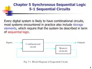
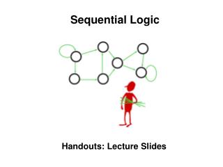
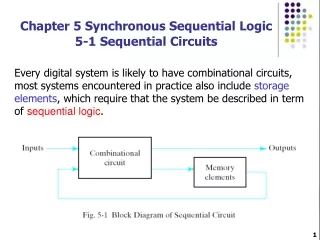
Sequential Logic • Outputs of sequential logic depend on current inputs and prior input values • Sequential logic might explicitly remember certain previous inputs, or it might distill (encode) the prior inputs into a smaller amount of information called state • The state is a set of bits that contain all the information about the past necessary to explain the future behavior of the circuit • State elements • Bistable circuit • SR Latch • D Latch • D Flip-flop
Bistable Circuit • Bistable circuit is the fundamental building block of other state elements • A pair of inverters are connected in a loop • Two outputs: Q, Q • No inputs
Bistable Circuit Analysis • Let’s consider the two possible cases • Q = 0: • Q = 1: then Q = 1 and Q = 0 (consistent) 1 1 0 then Q = 0 and Q = 1 (consistent) 0 0 1
Bistable Circuit Analysis • Bistable circuit stores 1 bit of state in the state variable • Q (or Q ) • But, there are no inputs to control the state • A subtle point is that the circuit could have a third possible state with both outputs approximately halfway between 0 and 1 (halfway between 0 and Vdd) • It is called a metastable state Vdd/2 Vdd/2 Vdd/2 Vdd/2
Bistable Circuit • Even though the cross-coupled inverters can store a bit of information, they are not practical because they don’t have inputs to control the state. • Other bistable elements such as latchesandflip-flopsprovide inputs to control the value of the state variable
SR Latch • One of the simplest sequential circuits is the SR (Set/Reset) latch • It is composed of 2 cross-coupled NOR gates • It has 2 inputs (S, R) and 2 outputs (Q and Q) • When the set input (S) is 1 (and R = 0), Q is set to 1 • Set makes the output (Q) to “1” • When the reset input (R) is 1 (and S = 0), Q is reset to 0 • Reset makes the output (Q) to “0”
SR Latch Analysis • Consider the four possible cases: a) S = 1, R = 0 b) S = 0, R = 1 c) S = 0, R = 0 d)S = 1, R = 1
SR Latch Analysis a) S = 1, R = 0: b)S = 0, R = 1: 1 then Q = 1 and Q = 0 0 1 0 then Q = 0 and Q = 1 0 1 0 1
SR Latch Analysis c) S = 0, R = 0: d) S = 1, R = 1: We got Memory! then Q = Qprev and Q = Qprev 1 0 1 0 1 0 1 0 Invalid state: Q≠ NOT Q 0 then Q = 0 and Q = 0 0 0 0
SR Latch Recap • SR latch stores one bit of state • Where is it stored? • SR latch can control the state with S, R inputs • SR latch generates the invalid state when S =1 and R = 1
D Latch • D latch solves the problem with SR latch • D latch blocks the invalid state when S =1 and R = 1 • D latch separates when and what the state should be changed • D latch has 2 inputs (CLK, D) and 2 outputs (Q, Q) • CLK controls when the output changes • D (data input) controls what the output changes to • Avoids invalid case (Q ≠ NOT Q when both S and R are 1)
D Latch Internal & Operation • D latch operation • When CLK = 1, D passes through to Q (D latch is transparent) • When CLK = 0, Q holds its previous value (D latch is opaque) 0 Qprev 1 0 0 0 1 1 0 1 0 1 Qprev Qprev Qprev 0 0 0 1 0 1 0 1 0 1 0 1 0
D Latch Waveform • When evaluating latch, it would be confusing if you think previous value and current value things • To get a good intuition, think with waveform • When CLK = 1, D latch transfers input data (D) to output (Q) • When CLK = 0, D latch maintains its previous value
D Flip-Flop • In digital logic design, it would be very convenient if we can store input data at a certain moment (not during the whole time interval like D latch) • D flip-flop provides that functionality • Q changes only on the rising edge of CLK • When CLK rises from 0 to 1, D passes through to Q • Otherwise, Q holds its previous value • Thus, a flip-flop is called an edge-triggered device because it is activated on the clock edge
D Flip-Flop Internal Circuit • Two back-to-back latches (L1 and L2) controlled by complementary clocks • When CLK = 0 • L1 is transparent • L2 is opaque • D passes through to N1 • When CLK = 1 • L2 is transparent • L1 is opaque • N1 passes through to Q • Thus, on the edge of the clock (when CLK rises from 0 to 1) • D effectively passes through to Q
D Flip-Flop • Note that input data should not be changed around the clock edge for D flip-flop to work correctly
D Flip-Flop • So, D flip-flop has the effect of sampling the current input data at the rising edge of the clock • Note that input data should not be changed around the clock edge for D flip-flop to work correctly
Registers • An N-bit register is a bank of N flip-flops that share a common CLK input, so that all bits of the register are updated at the same time • You can say N-bit flip-flops or N-bit register • Registers are the key building block of sequential circuits
Flip-Flops • There are several kinds of flip-flops • Enabled flip-flops • Resettable flip-flops • Settable flip-flops • These flip-flops and just plain flip-flops are used extensively in the digital design • You will use these flip-flops when designing CPU in the next semester
Enabled Flip-Flops • Enabled flip-flips are useful when we wish to load a new value into a flip-flop only during some of the time, rather than on every clock edge • Enabled flip-flop has one more input (EN) • The enable input (EN) controls when new data (D) is stored • When EN = 1, D passes through to Q on the clock edge • When EN = 0,the flip-flop retains its previous state
Resettable Flip-Flops • Resettable flip-flops are useful when we want to force a known state (i.e., 0) into some flip-flops in a system when we first turn it on • Resettable flip-flop has “Reset” input • When Reset = 1, Q is reset to 0 • When Reset = 0, the flip-flop behaves like an ordinary D flip-flop • There are two types of resettable flip-flops • Synchronousresettable FF resets at the clock edge only • Asynchronousresettable FF resets immediately when Reset = 1 • Asynchronously resettable flip-flop requires changing the internal circuitry of the flip-flop Resettable flip-flop Synchronously resettable flip-flop
Settable Flip-Flops • Settable flip-flops are also useful when we want to force a known state (i.e., 1) into some flip-flops in a system when we first turn it on • Settable flip-flop has “Set” input • When Set = 1, Q is set to 1 • When Set = 0, the flip-flop behaves like an ordinary D flip-flop