Download
1 / 1
10 likes | 129 Views
Stability of Tensile-strained Ge Studied by Transmission Electron Microscopy. Daniel C. Ralph, Cornell University, ECCS 0335765.

E N D
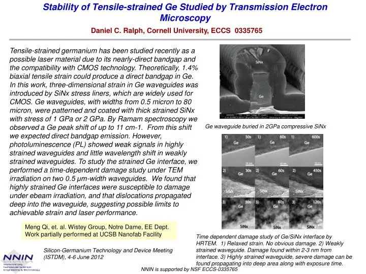
Stability of Tensile-strained Ge Studied by Transmission Electron Microscopy Daniel C. Ralph, Cornell University, ECCS 0335765 Tensile-strained germanium has been studied recently as a possible laser material due to its nearly-direct bandgap and the compatibility with CMOS technology. Theoretically, 1.4% biaxial tensile strain could produce a direct bandgap in Ge. In this work, three-dimensional strain in Ge waveguides was introduced by SiNx stress liners, which are widely used for CMOS. Ge waveguides, with widths from 0.5 micron to 80 micron, were patterned and coated with thick strained SiNx with stress of 1 GPa or 2 GPa. By Ramam spectroscopy we observed a Ge peak shift of up to 11 cm-1. From this shift we expected direct bandgap emission. However, photoluminescence (PL) showed weak signals in highly strained waveguides and little wavelength shift in weakly strained waveguides. To study the strained Ge interface, we performed a time-dependent damage study under TEM irradiation on two 0.5 μm-width waveguides. We found that highly strained Ge interfaces were susceptible to damage under ebeam irradiation, and that dislocations propagated deep into the waveguide, suggesting possible limits to achievable strain and laser performance. Ge waveguide buried in 2GPa compressive SiNx Meng Qi, et. al. Wistey Group, Notre Dame, EE Dept. Work partially performed at UCSB Nanofab Facility Time dependent damage study of Ge/SiNx interface by HRTEM. 1) Relaxed strain. No obvious damage. 2) Weakly strained waveguide. Damage found within 2-3 nm from interface. 3) Highly strained waveguide, severe damage can be found propagating into deep area along with exposure time. Silicon-Germanium Technology and Device Meeting (ISTDM), 4-6 June 2012