Download
1 / 68
900 likes | 1.36k Views
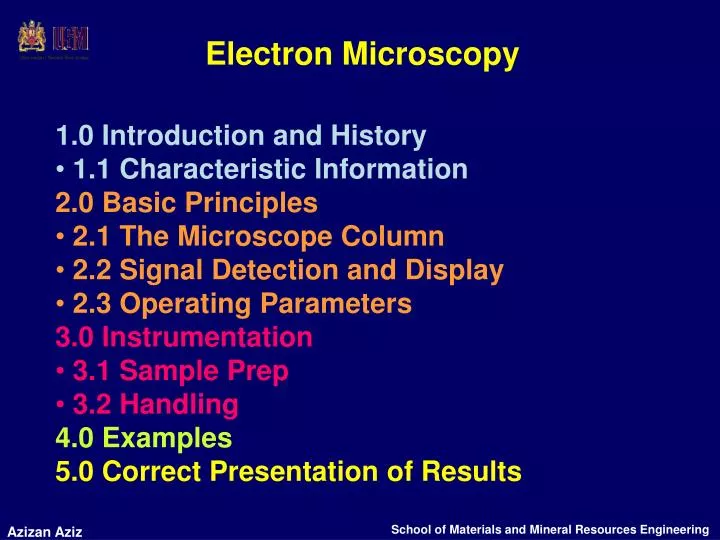
Electron Microscopy. 1.0 Introduction and History • 1.1 Characteristic Information 2.0 Basic Principles • 2.1 The Microscope Column • 2.2 Signal Detection and Display • 2.3 Operating Parameters 3.0 Instrumentation • 3.1 Sample Prep • 3.2 Handling 4.0 Examples

E N D
Electron Microscopy 1.0 Introduction and History • 1.1 Characteristic Information 2.0 Basic Principles • 2.1 The Microscope Column • 2.2 Signal Detection and Display • 2.3 Operating Parameters 3.0 Instrumentation • 3.1 Sample Prep • 3.2 Handling 4.0 Examples 5.0 Correct Presentation of Results
Scanning Electron Microscope (SEM) and Microprobe Electron microscopy takes advantage of the wave nature of high speed electrons In an SEM, the sample surface is swept in a raster pattern with a finely focussed beam of electrons. Visible light wavelength: 4000 - 7000 Å electrons accelerated to 10,000 keV have a wavelength of 0.12 Å EM provides much higher diffraction limited resolution Physical nature of a solid surface: scanning electron microscopy (SEM) Chemical composition of surface: analytical electron microscopy (AEM) Most modern electron microscopes are designed to perform both types of measurements
1.0 Introduction and History What are they and Where did Electron Microscopes Come From? Electron Microscopes are scientific instruments that use a beam of highly energetic electrons to examine objects on a very fine scale. Electron Microscopes were developed due to the limitations of Light Microscopes which are limited by the physics of light to 500x or 1000x magnification and a resolution of 0.2 mm.
1.0 Introduction and History (continue) In the early 1930's this theoretical limit had been reached and there was a scientific desire to see the fine details of the interior structures of organic cells (nucleus, mitochondria...etc.). This required 10,000x plus magnification which was just not possible using current optical microscopes.
Dates The Transmission Electron Microscope (TEM) was the first type of Electron Microscope to be developed and is patterned exactly on the Light Transmission Microscope except that a focused beam of electrons is used instead of light to "see through" the specimen. It was developed by Max Knoll and Ernst Ruska in Germany in 1931. The first Scanning Electron Microscope (SEM) debuted in 1938 ( Von Ardenne) with the first commercial instruments around 1965. Its late development was due to the electronics involved in "scanning" the beam of electrons across the sample.
Chronology 1897: J.J. Thompson - Discovers the electron 1924: Louis deBroglie Identifies a wavelength to moving electrons - = h / mv where: = wavelength, h = Planck's constant m = mass, v = velocity (For an electron at 60kV, = 0.005 nm) 1926: H. Busch - Magnetic or electric fields act as lenses for electrons 1929: E. Ruska - Ph.D thesis on magnetic lenses 1931: Knoll & Ruska - First electron microscope built 1931: Davisson & Calbrick - Properties of electrostatic lenses 1934: Driest & Muller - Surpass resolution of the OM 1938: von Borries & Ruska First practical EM (Siemens) - 10 nm resolution 1940: RCA - Commercial EM with 2.4 nm resolution
Microscopy and Related Techniques • Light (optical) microscopy (LM) or (OM) • Scanning electron microscopy (SEM) Energy dispersive X-ray spectroscopy (EDS) & Wavelength dispersive X-ray spectroscopy (WDS) • X-ray diffraction (XRD)/X-ray fluorescence (XRF) • Transmission electron microscopy/Scanning transmission electron microscopy (TEM)/(STEM) Surface Characterization Techniques Scanning probe microscopy (AFM & STM)
1.1 Characteristic Information • Topography • The surface features of an object or "how it looks", its texture; direct relation between these features and materials properties 2. Morphology The shape and size of the particles making up the object;direct relation between these structures and materials properties 4.Crystallographic Information How the atoms are arranged in the object; direct relation between these arrangements and materials properties 3. Composition The elements and compounds that the object is composed of and the relative amounts of them; direct relationship between composition and materials properties
Identification of Fracture Mode SEM micrographs of fractured surface of two BaTiO3 samples.
How Fine can You See? • Can you see a sugar cube? The thickness of a sewing needle? The thickness of a piece of paper? … • The resolution of human eyes is of the order of 0.1 mm, 100mm » 4 mils. • However, something vital to human beings are of sizes smaller than 0.1mm, e.g. our cells, bacteria, microstructural details of materials, etc.
Microstructural Features which Concern Us • Grain size: from <mm to the cm regime • Grain shapes • Precipitate size: mostly in the mm regime • Volume fractions and distributions of various phases • Defects such as cracks and voids: <mm to the cm regime
Phase Contrast Microscopy - Phase contrast microscopy, first described in 1934 by Dutch physicist Frits Zernike, is a contrast-enhancing optical technique that can be utilized to produce high-contrast images of transparent specimens such as living cells, microorganisms, thin tissue slices, lithographic patterns, and sub-cellular particles (such as nuclei and other organelles).
In effect, the phase contrast technique employs an optical mechanism to translate minute variations in phase into corresponding changes in amplitude, which can be visualized as differences in image contrast. One of the major advantages of phase contrast microscopy is that living cells can be examined in their natural state without being killed, fixed, and stained. As a result, the dynamics of ongoing biological processes in live cells can be observed and recorded bin high contrast with sharp clarity of minute specimen detail.
Scale and Microscopy Techniques Microstructure ranging from crystal structure to Engine components (Si3N4)
Advantages of Using SEM over OM The SEM has a large depth of field, which allows a large amount of the sample to be in focus at one time and produces an image that is a good representation of the three-dimensional sample. The SEM also produces images of high resolution, which means that closely features can be examined at a high magnification.
The combination of higher magnification, larger depth of field, greater resolution and compositional and crystallographic information makes the SEM one of the most heavily used instruments in research areas and industries, especially in semiconductor industry.
The Microscope Column General Layout In simplest terms, an SEM is really nothing more than a television. We use a filament to get electrons, magnets to move them around, and a detector acts like a camera to produce an image.
Scanning Electron Microscope 1) The "Virtual Source" at the top represents the electron gun, producing a stream of monochromatic electrons. 2) The stream is condensed by the first condenser lens (usually controlled by the "coarse probe current knob"). This lens is used to both form the beam and limit the amount of current in the beam. It works in conjunction with the condenser aperture to eliminate the high-angle electrons from the beam.
3) The beam is then constricted by the condenser aperture (usually not user selectable), eliminating some high-angle electrons. 4) The second condenser lens forms the electrons into a thin, tight, coherent beam and is usually controlled by the "fine probe current knob". 5) A user selectable objective aperture further eliminates high-angle electrons from the beam.
6) A set of coils then "scan" or "sweep" the beam in a grid fashion (like a television), dwelling on points for a period of time determined by the scan speed (usually in the microsecond range). 7) The final lens, the Objective, focuses the scanning beam onto the part of the specimen desired. 8) When the beam strikes the sample (and dwells for a few microseconds) interactions occur inside the sample and are detected with various instruments.
9) Before the beam moves to its next dwell point these instruments count the number of interactions and display a pixel on a CRT whose intensity is determined by this number (the more reactions the brighter the pixel). 10) This process is repeated until the grid scan is finished and then repeated, the entire pattern can be scanned 30 times/sec.
Parts of the Microscope 1. Electron optical column consists of: – electron source to produce electrons – magnetic lenses to de-magnify the beam – magnetic coils to control and modify the beam – apertures to define the extent of beam, prevent electron spray, etc. 2. Vacuum systems consists of: – chamber which “holds” vacuum – pumps to produce vacuum – valves to control vacuum – gauges to monitor vacuum 3. Signal Detection & Display consists of: – detectors which collect the signal – electronics which produce an image from the signal
Getting a Beam • A filament is heated to a high T to emit electrons. • A bias (of up to 45 kV) between the filament and a target material draws the electrons to an anode. • Up to this point, the process is identical to that used to form x-rays. However, instead of striking a target to form x-rays, the electrons are drawn towards an anode, where they go through a hole, forming a beam. • This beam is attracted through the anode, condensed by a condenser lens, and focused as a very fine point on the sample by the objective lens.
Electron Beam Source W / LaB6 (Filament) Thermionic or Cold Cathode (Field Emission Gun)
Field Emission Gun • The tip of a tungsten needle is made very sharp (radius < 0.1 mm) • The electric field at the tip is very strong (> 107 V/cm) due to the sharp point effect • Electrons are pulled out from the tip by the strong electric field • Ultra-high vacuum (better than 10-6 Pa) is needed to avoid ion bombardment to the tip from the residual gas. • Electron probe diameter < 1 nm is possible
Electromagnetic Lenses Lorentz force equation: F = q0v x B Nonaxial electrons will experience a force both down the axis and one radial to it. Only electrons traveling down the axis feel equal radial forces from all sides of the lens. The unequal force felt by the off-axis electronscauses spiraling about the optic axis. Two components to the B field: BL = longitudinal component (down the axis) BR= radial component (perpendicular to axis)
Electromagnetic Lenses • Condenser lens – focusing determines the beam current which impinges on the sample. • Objective lens – final probe forming • The objective lens determines the final spot size of the electron beam, i.e., the resolution of a SEM. The Condenser Lens • For a thermionic gun, the diameter of the first crossover point ~20-50µm. • If we want to focus the beam to a size < 10 nm on the specimen surface, the magnification should be ~1/5000, which is not easily attained with one lens (say, the objective lens) only. • Therefore, condenser lenses are added to demagnify the cross-over points.
The Objective Lens • The objective lens controls the final focus of the electron beam by changing the magnetic field strength • The cross-over image is finally demagnified to an ~10nm beam spot which carries a beam current of approximately 10-9 - 10-13 A.
The Objective Lens - Focusing By changing the current in the objective lens, the magnetic field strength changes and therefore the focal length of the objective lens is changed.
The Objective Lens - Stigmator • The objective lens is machined to very high precision and the magnetic field pattern is very carefully designed. • However, the precision attainable by machining cannot match that required for controlling a beam with a 10 nm diameter. • The stigmator, which consist of two pairs of pole-pieces arranged in the X and Y directions, is added to correct the minor imperfectionsin the objective lens.
The Objective Lens - Aperture • Since the electrons coming from the electron gun have spread in kinetic energies and directions of movement, they may not be focused to the same plane to form a sharp spot. • By inserting an aperture, the stray electrons are blocked and the remaining narrow beam will come to a narrow “Disc of Least Confusion”
Electron vs. Optical Lenses • e-’s don’t actually touch the lens - No definite interface • e-’s rotate in the magnetic field • e-’s repel each other • f H I - Focus and magnification controlled electronically - No physical movements • e- lenses can only be positive elements (converging) • Can’t correct e- lens aberrations like you can with compound optical lenses • e- lenses always operate at small apertures
Comparison of OM,TEM and SEM Principal features of an optical microscope, a transmission electron microscope and a scanning electron microscope, drawn to emphasize the similarities of overall design.
Signal Detection and Display When an electron beam strikes a sample, a large number of signals are generated. We can divide the signals into two broad categories: a) electron signals, b) photon signals
Electron Detectors and Sample Stage Sample Stage
Specimen Interaction Volume The volume inside the specimen in which interactions occur while being struck with an electron beam. Thisvolume depends on the following factors: • • Atomic number of the material being examined; higher atomic number materials absorb or stop more electrons and so have a smaller interaction volume. • • Accelerating voltage: higher voltages penetrate farther into the sample and generate larger interaction volumes • • Angle of incidence for the electron beam; the greater the angle (further from normal) the smaller the volume
Specimen Interaction Volume • Below is an example of a typical Interaction volume for: • Specimen with atomic number 28, 20 kV • 0° degrees tilt, incident beam is normal to specimen surface noting the approximate maximum sampling depths for the
Signal Detection and Display • If you change the target material, the high and low energy peaks remain (although their intensity may change) while the low intensity peaks change position and are characteristic of the sample. • The reason we produce this type of profile is because the incident electrons we send into the sample are scattered in different ways. • There are two broad categories to describe electron scattering: – elastic: Backscattered electrons – inelastic: Secondary electrons
Secondary Electrons These electrons arise due to inelastic collisions between primary electrons (the beam) and loosely bound electrons of the conduction band (more probable) or tightly bound valence electrons. The energy transferred is sufficient to overcome the work function which binds them to the solid and they are ejected. The interaction is Coulombic in nature and the ejected electrons typically have ˜ 5 - 10 eV. 50 eV is an arbitrary cut-off below which they are said to be secondary electrons.
Detection Remember, secondary electrons are low energy electrons. We can easily collect them by placing a positive voltage (100 - 300V) on the front of our detector. Since this lets us collect a large number of the secondaries (50 - 100%), we produce a “3D” type of image of the sample with a large depth of field. The type of detector used is called a scintillator / photomultiplier tube.
Detection Sequence • Secondary electrons (SE) are accelerated to the front of the detector by a bias voltage of 100 - 500 eV. • 2. They are then accelerated to the scintillator by a bias of 6 - 12 keV, (10KeV is normal).