Download
1 / 45
460 likes | 651 Views
2009 Topical Workshop on Heterostructure Microelectronics, August 25-28, Nagano, Japan,. Process Technologies For Sub-100-nm InP HBTs & InGaAs MOSFETs. Mark. Rodwell, University of California, Santa Barbara.

E N D
2009 Topical Workshop on Heterostructure Microelectronics, August 25-28, Nagano, Japan, Process Technologies For Sub-100-nm InP HBTs & InGaAs MOSFETs Mark. Rodwell, University of California, Santa Barbara M. A. Wistey*, U. Singisetti, G. J. Burek, B. J. Thibeault, A. Baraskar, E. Lobisser, V. Jain, J. Cagnon, S. Stemmer, A. C. GossardUniversity of California, Santa Barbara*Now at Notre Dame E. Kim, P. C. McIntyreStanford University Y.-J. LeeIntel B. Yue, L. Wang, P. Asbeck, Y. TaurUniversity of California, San Diego
III-V transistors: the goal is scaling 2-3 THz InP HBTs: 32 nm / 64 nm scaling generations 2-3 THz HEMTs: 10-15 nm, balanced / fully scaled devices 15 nm InGaAs MOSFETs for VLSI implication: we need new fabrication processes
Changes required to double transistor bandwidth nearly constant junction temperature → linewidths vary as (1 / bandwidth)2 fringing capacitance does not scale → linewidths scale as (1 / bandwidth ) constant voltage, constant velocity scaling
III-V Fabrication Processes Must Change... Greatly 32 nm base & emitter contacts...self-aligned 32 nm emitter junctions 1 W-mm2 contact resistivities 70 mA/mm2 → refractory contacts 15 nm gate length 15 nm source / drain contacts...self-aligned < 10 nm source / drain spacers (sidewalls) 1/2 W-mm2 contact resistivities 3 mA/mm→ 200 mA/mm2 contacts above ~ 5 nm N+ layer→ refractory contacts !
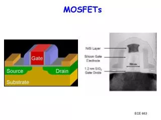
Why III-V MOSFETs • Silicon MOSFETs: • Gate oxide may limit <16 nm scaling Id / Wg ~ cox(Vg-Vth)vinj IBM 45nm NMOS Narayan et al, VLSI 2006 Alternative: In0.53Ga0.47As channel MOSFETs low m* (0.041 mo) → high injection velocity, vinj (~ 2-3×107 cm/s)* →increase drive current, decreased CV/I * Enoki et al , EDL 1990
double the MOSFET speed keep constant gate control vertical scaling tox , tqw , xj MOSFET scaling*: lateral and vertical Goal : double package density → lateral scaling Lg, Wg, Ls/d *Rodwell, IPRM 2008
Target device structure Target 22 nm gate length Control of short-channel effects vertical scaling 1 nm EOT: thin gate dielectric, surface-channel device 5 nm quantum well thickness <5 nm deep source / drain regions ~3 mA/mm target drive current low access resistance self-aligned, low resistivity source / drain contacts self-aligned N+ source / drain regions with high doping
22 nm InGaAs MOSFET: Source Resistance Lg LS/D IBM High-k Metal gate transistor Image Source: EE Times • Source access resistance degrades Id and gm • IC Package density : LS/D ~ Lg =22 nm → rc must be low • Need low sheet resistance in thin ~5 nm N+ layer • Design targets: rc ~1 W-mm2, rsheet ~ 400 W
22nm ion implanted InGaAs MOSFET Key Technological Challenges • Shallow junctions ( ~ 5 nm), high (~5×1019 cm-3)doping • Doping abruptness ( ~ 1 nm/decade) • Lateral Straggle ( ~ 5 nm) • Deep junctions would lead to degraded short channel effects
Gate Source Drain Why HEMTs are Hard to Improve 1st challenge with HEMTs: reducing access resistance low electron density under gate recess→ limits current gate barrier lies under S/D contacts → resistance gate barrier channel K Shinohara 2nd challenge with HEMTs: low gate barrier high tunneling currents with thin barrier high emission currents with high electron density III-V MOSFETs do not face these scaling challenges
HEMTs Differ in Access Resistance, Electrostatics HEMTs: short gate lengths, wide spacing / recess, wide contacts wide recess→ improved DIBL, improved subthreshold slope, wide contacts→ OK access resistivity even with poor contacts VLSI MOSFETs : short gate lengths, narrow contacts, no spacing/recess Need good DIBL even with zero drain/gate offset. Need low S/D resistance even with 22 nm width contacts.
InGaAs MOSFET with N+ Source/Drain by MEE Regrowth1 HAADF-STEM1* InGaAs regrowth Interface InGaAs 2 nm * TEM by J. Cagnon, Susanne Stemmer Group, UCSB Self-aligned source/drain defined by MBE regrowth2 Self-aligned in-situ Mo contacts3 Process flow & dimensions selected for 22 nm Lg design; present devices @ 200 nm gate length 1Singisetti, ISCS 2008 2Wistey, EMC 2008 3Baraskar, EMC 2009
Regrown S/D process: key features Self-aligned & low resistivity ...source / drain N+ regions ...source / drain metal contacts Vertical S/D doping profile set by MBE no n+ junction extension below channel abrupt on few-nm scale Gate-first gate dielectric formed after MBE growth uncontaminated / undamaged surface
Process flow* * Singisetti et al, 2008 ISCS, September, Frieburg Singisetti et al; Physica Status Solidi C, vol. 6, pp. 1394,2009
Key challenge in S/D process: gate stack etch Requirement: avoid damaging semiconductor surface: Approach: Gate stack with multiple selective etches* FIB Cross-section Damage free channel SiO2 Cr W Process scalable to sub-100 nm gate lengths * Singisetti et al; Physica Status Solidi C, vol. 6, pp. 1394,2009
Key challenge in S/D process: dielectric sidewall spillover ns under sidewall: electrostatic spillover from source, gate Sidewall must be kept thin: avoid carrier depletion, avoid source starvation 2-DSimulation of an artificially on state device in Atlas, Silvaco. Source doping 6e19 cm-3
Raised vs. Recessed S/D Regrowth: planar regrowth regrowth under sidewalls more difficult growth... ...tolerate of high Dit in access region need thin sidewalls (now ~25nm) High Dit ?→ severe carrier depletion SRC Neoclassical CMOS Research Center
MBE Regrowth→ Gap Near Gate→ Source Resistance Ti/Au Pad SiO2 cap SEM Mo+InGaAs W / Cr / SiO2 gate W/Cr gate Gap in regrowth SEM • Shadowing by gate: No regrowth next to gate • Gap region is depleted of electrons W / Cr / SiO2 gate High source resistance because of electron depletion in the gap MBE growth by Dr. Mark Wistey, device fabrication and characterization by U. Singisetti
Migration Enhanced Epitaxial (MEE) S/D Regrowth* High T migration enhanced Epitaxial (MEE) regrowth* 45o tilt SEM No Gap Top of SiO2 gate gate Side of gate regrowth interface No Gap High temperature migration enhanced epitaxial regrowth *Wistey, EMC 2008 Wistey, ICMBE 2008 MBE growth by Dr. Mark Wistey, device fabrication and characterization by U. Singisetti
Regrown S/D III-V MOSFET: Images Cross-section after regrowth, but before Mo deposition Top view of completed device
Source Resistance: electron depletion near gate R1 R2 • Electron depletion in regrowth shadow region (R1 ) • Electron depletion in the channel under SiNx sidewalls (R2 )
Regrowth profile dependence on As flux* SiO2 InAlAs InGaAs InGaAs increasingAs flux Cr InGaAs W InGaAs regrowth surface uniform filling multiple InGaAs regrowths with InAlAs marker layers Uniform filling with lower As flux * Wistey et al, EMC 2009 Wistey et al NAMBE 2009 MBE growth by Dr. Mark Wistey, device fabrication and characterization by U. Singisetti
InAsregrowth Gate InAs source/drain regrowth top of gate side of gate Mo S/D metal with N+ InAs underneath Improved InAs regrowth with low As flux for uniform filling1 InAs less susceptible to electron depletion: Fermi pinning above Ec2 1 Wistey et al, EMC 2009 Wistey et al NAMBE 2009. 2Bhargava et al , APL 1997
Dummy gate No regrowth Self-Aligned Contacts: Height Selective Etching* PR Mo PR PR InGaAs * Burek et al, J. Cryst. Growth 2009
Why Is the Device Drive Current Low ? → Dit Devices used Stanford / McIntyre ALD Al2O3 gate dielectric best Stanford results: H passivation for low Dit. FET results: H gets driven away in process need, but do not yet have, post-process H anneal → high Dit on present FETs, c.a. 1013 / cm2/eV. High Dit → Carrier depletion under sidewalls greatly increased access resistance. High Dit→ inefficient charge modulation→ low gm.
150 nm thick collector 256 nm GenerationInP DHBT 70 nm thick collector 324 GHzAmplifier 60 nm thick collector 200 GHz master-slavelatch design Z. Griffith, E. Lind J. Hacker, M. Jones
Process Must Change Greatly for 128 / 64 / 32 nm Nodes control undercut→ thinner emitter thinner emitter→ thinner base metal thinner base metal→ excess base metal resistance Undercutting of emitter ends... ...and loss of emitter adhesion. {101}A planes: fast {111}A planes: slow
128 / 64 nm HBT Process: Where We Are Going Key Features: contact metals: no liftoff sputter deposition dry etched ohmic contacts base & emitter refractory: thermally stable semiconductor junctions dry etchedself-aligned target ~2000 GHz device
Fabrication Processes for nm/THz III-V Transistors 10-30 nm junctions ... ~1 W-mm2 contact resistivities ~100 mA/mm2 current densities refractory contacts sputter-deposited dry-etched self-alignment: dielectric sidewall spacers height-selective etching dry-etched junctions, minimal wet-etching
Subthreshold characteristics • Ion/Ioff~ 104:1
Why do we need base regrowth? Regrowth for less resistive base contacts contact moved away from c/b junction better reliability with thin base layers Migration Enhanced Epitaxial Regrowth dummy emitter no gap regrowth interface p =5x1019 cm-3 , m=15 cm2/Vs
Bipolar Transistor Scaling Laws Changes required to double transistor bandwidth: Linewidths scale as the inverse square of bandwidth because thermal constraints dominate.
industry university→industry university2007-8 appearsfeasible maybe InP Bipolar Transistor Scaling Roadmap emitter 512 256 128 64 32 nm width16 8 4 2 1 m2 access r base 300 175 120 60 30 nm contact width, 20 10 5 2.5 1.25 m2 contact r collector 150 106 75 53 37.5 nm thick, 4.5 9 18 36 72 mA/m2 current density 4.9 4 3.3 2.75 2-2.5 V, breakdown ft 370 520 730 1000 1400 GHz fmax 490 850 1300 2000 2800 GHz power amplifiers 245 430 660 1000 1400 GHz digital 2:1 divider 150 240 330 480 660 GHz
THz / nm Transistors: it's all about the interfaces Metal-semiconductor interfaces (Ohmic contacts):very low resistivity Dielectric-semiconductor interfaces (Gate dielectrics):very high capacitance density Transistor & IC thermal resistivity.
FET Scaling Laws Changes required to double transistor bandwidth: Linewidths scale as the inverse of bandwidth because fringing capacitance does not scale.
Goal double transistor bandwidth when used in any circuit → reduce 2:1 all capacitances and all transport delays→ keep constant all resistances, voltages, currents Simple FET Scaling All lengths, widths, thicknesses reduced 2:1 S/D contact resistivity reduced 4:1 If Tox cannot scale with gate length, Cparasitic / Cgs increases, gm / Wg does not increasehence Cparasitic /gm does not scale