Download
1 / 28
360 likes | 1.38k Views
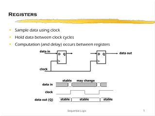
Registers. A register is a group of n flip-flops each of them capable of storing one bit of information There are two types of registers: parallel and serial registers. They differ in the manner in which the binary data is loaded and retrieved from them. 4-Bit Register.

E N D
Registers A register is a group of n flip-flops each of them capable of storing one bit of information There are two types of registers: parallel and serial registers. They differ in the manner in which the binary data is loaded and retrieved from them A.Abhari CPS213
4-Bit Register • 4-bit register constructed with four positive edge-triggered D-type flip-flops with parallel load. • Positive-edge-triggered D flip flop responses (i.e., value of D transfers to Q) only to the transition from 0 to 1 and nothing else • The positive-edge-triggered D flip flop that is used in a 4-bit register has also additional direct reset input named CLEAR or RESET. When CLEAR is 0 the flip flop is resetting independent of clock and D values. It is useful because in digital systems when the power is turned on the state of flip-flops is unknown. Direct input CLEAR can bring all flip-flops to the known starting state prior to the clock operation. Next slid shows positive-edge-D flip flop with asynchronous reset. A.Abhari CPS213
Register with Parallel load • If all bits of the register are loaded simultaneously with a common clock pulse, we say that the loading is done in parallel • When we want some registers remain unchanged (even with clock changes) we can use a load control input (see the next slide) • The load input determines whether the next pulse will accept new information or leave the information in the register intact. A.Abhari CPS213
4-bit Parallel Register • 4-bit parallel register can be implemented with negative-edge-triggered-DFF as well. Here is the review of the graphic symbols for positive and negative edge-triggered DFF A.Abhari CPS213
Writing in the 4-bit Parallel Register • Circuit uses a series of negative-edge-triggered-DFF • The clock input to all flip-flops are connected to active-low write line (WR) • The flip flops are triggered when WR line changes to logic 0 • See the figure presented in the class A.Abhari CPS213
Reading and Writing in 4-bit Parallel Register with tri-state output • By adding active low read line (RD) the output of register can be read • We can use tri-state buffers (enable with logic 0) connected to each output line to be able to put output on the bus when we need • If RD is inactive (logic 1 state ) the outputs of registers are in high-impedance (Z) state and register can be load with input line so by changing WR to 0 the input written in register. • When RD is active (logic 0 state) by keeping WR line inactive, buffers are active and output of FFs can be read. Can not R and W in the same time. • See the figure presented in the class A.Abhari CPS213
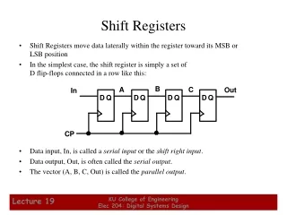
Shift Register • A register capable of shifting its binary information in one or both directions is called a shift register • For example by connecting the output of each D flip-flop to the input of another D flip flop in its right, each clock pulse shifts the content of the register one bit position to the right. The serial input determines what goes into the leftmost flip flop during the shift. The serial output is taken from the output of the rightmost flip flop. A.Abhari CPS213
A.Abhari CPS213
Serial Transfer The difference between serial transfer and parallel transfer is: • In the parallel mode information is available from all bits of register and all bits can be transferred simultaneously during one clock pulse. • In the serial mode, the registers have a single serial input and a single serial output. The information is transferred one bit at a time while registers are shifted in the same direction A.Abhari CPS213
Serial Transfer • For example next slide shows the serial transfer from register A to register B by using shift register • To prevent the loss of information stored in the source register the serial output of A is connected to its serial input • The shift control input determines when and how many times the register are shift. Here each register has four bits and each rising edge of the pulse cause a one bit shift in each register. For a fixed time of four clock pulses the content of A is transferred into B, while the contents of A remains unchanged. A.Abhari CPS213
Ripple Counters • A register goes through a prescribed sequence of states upon the application of input pulses is called counter • An n bit binary counter consists of n flip-flops and can count 2n – 1 • Asynchronous counters don’t have common clock connected to their C input. Next slide shows Asynchronous 4-bit binary counter A.Abhari CPS213
Ripple Counters • When using DFF for binary counter the complement output connected to D input to make sure D input is always the complement of the present state, therefore the next pulse will cause the FF to complement • BCD ripple counter follows same sequence but returns to 0 after counting to 9. See next two slides A.Abhari CPS213
A.Abhari CPS213
Counts from 0 to 999 A.Abhari CPS213
3-Bit Binary Counter • In the synchronous counters clock pulses are applied to the input of all flip-flops • For designing a 3-bit counter we can simply follow the design procedure for sequential circuits • First we design state diagram and then by finding state table and flip-flop equations we design the circuit (see next three slides) A.Abhari CPS213
A.Abhari CPS213
A1A0 A2 A.Abhari CPS213
A.Abhari CPS213
Synchronous Counter • In synchronous binary counter, the flip-flop in the least significant position is complemented with every pulses. Also each FF is complemented when all FFs in the lower significant positions are equal to 1. • For example in the next slide A0 is always complemented. A1 is complemented when the present state of A0 is 1. A2 is complemented when present state of A1A0=11. A3 is complemented when present state of A2A1A0=111. • By using this pattern we can design 4 bit synchronous counter easier than going through the sequential design process. (see next slides) A.Abhari CPS213
Up-Down Binary Counter • A synchronous count down binary counter goes through the binary states in the reverse order from 1111 down to 0000 and back to 1111 • The least significant bit is always complemented. Each bit is complemented if all the lower bits are equal to 0 • The two operations can be combined in one circuit to form a counter capable of counting either up or down • When up and down inputs are 0, the circuit does not change state and when there are both 1, the circuit counts up. A.Abhari CPS213