Download

1 / 26

E N D
MODULE 4 Registers
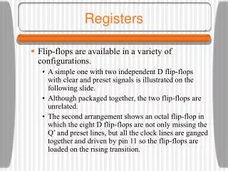
SHIFT REGISTERS • Introduction : • Shift registers are a type of sequential logic circuit, mainly for storage of digital data. They are a group of flip-flops connected in a chain so that the output from one flip-flop becomes the input of the next flip-flop. Most of the registers possess no characteristic internal sequence of states. All the flip-flops are driven by a common clock, and all are set or reset simultaneously.In this chapter, the basic types of shift registers are studied, such as Serial In - Serial Out, Serial In - Parallel Out, Parallel In - Serial Out, Parallel In - Parallel Out, and bidirectional shift registers. A special form of counter - the shift register counter, is also introduced.
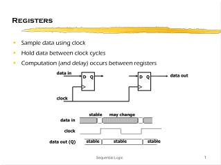
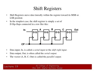
Serial In - Serial OutShift Registers • A basic four-bit shift register can be constructed using four D flip-flops, as shown below. The operation of the circuit is as follows. The register is first cleared, forcing all four outputs to zero. The input data is then applied sequentially to the D input of the first flip-flop on the left (FF0). During each clock pulse, one bit is transmitted from left to right. Assume a data word to be 1001. The least significant bit of the data has to be shifted through the register from FF0 to FF3.
Serial In - Serial OutShift Registers • In order to get the data out of the register, they must be shifted out serially. This can be done destructively or non-destructively. For destructive readout, the original data is lost and at the end of the read cycle, all flip-flops are reset to zero.
Serial In - Serial OutShift Registers • To avoid the loss of data, an arrangement for a non-destructive reading can be done by adding two AND gates, an OR gate and an inverter to the system. The construction of this circuit is shown below
Serial In - Serial OutShift Registers • The data is loaded to the register when the control line is HIGH (ie WRITE). The data can be shifted out of the register when the control line is LOW (ie READ). This is shown in the animation below.
Serial In - Parallel OutShift Registers • For this kind of register, data bits are entered serially in the same manner as discussed in the last section. The difference is the way in which the data bits are taken out of the register. Once the data are stored, each bit appears on its respective output line, and all bits are available simultaneously. A construction of a four-bit serial in - parallel out register is shown below.
Serial In - Parallel OutShift Registers • In the animation below, we can see how the four-bit binary number 1001 is shifted to the Q outputs of the register.
Parallel In - Serial OutShift Registers • A four-bit parallel in - serial out shift register is shown below. The circuit uses D flip-flops and NAND gates for entering data (ie writing) to the register.
Parallel In - Serial OutShift Registers • D0, D1, D2 and D3 are the parallel inputs, where D0 is the most significant bit and D3 is the least significant bit. To write data in, the mode control line is taken to LOW and the data is clocked in. The data can be shifted when the mode control line is HIGH as SHIFT is active high. The register performs right shift operation on the application of a clock pulse, as shown in the animation below.
Parallel In - Parallel OutShift Registers • For parallel in - parallel out shift registers, all data bits appear on the parallel outputs immediately following the simultaneous entry of the data bits. The following circuit is a four-bit parallel in - parallel out shift register constructed by D flip-flops.
Parallel In - Parallel OutShift Registers • The D's are the parallel inputs and the Q's are the parallel outputs. Once the register is clocked, all the data at the D inputs appear at the corresponding Q outputs simultaneously.
Bidirectional Shift Registers • The registers discussed so far involved only right shift operations. Each right shift operation has the effect of successively dividing the binary number by two. If the operation is reversed (left shift), this has the effect of multiplying the number by two. With suitable gating arrangement a serial shift register can perform both operations.A bidirectional, or reversible, shift register is one in which the data can be shift either left or right. A four-bit bidirectional shift register using D flip-flops is shown below.
Bidirectional Shift Registers • Here a set of NAND gates are configured as OR gates to select data inputs from the right or left adjacent bistables, as selected by the LEFT/RIGHT control line. • The animation below performs right shift four times, then left shift four times. Notice the order of the four output bits are not the same as the order of the original four input bits. They are actually reversed!
Shift Register Counters • Two of the most common types of shift register counters are introduced here: the Ring counter and the Johnson counter. They are basically shift registers with the serial outputs connected back to the serial inputs in order to produce particular sequences. These registers are classified as counters because they exhibit a specified sequence of states.
Universal Shift Register • Question: Design a Universal Shift Register with the following capabilities: • A clear control to clear the register to 0 • A clock to synchronize the operations • A shift-right control (associated with serial in/out) • A shift-left control (associated with serial in/out) • A parallel-load control (to parallel load n bits) • n-parallel output lines • A control signal to leave register unchanged Ahmad Almulhem, KFUPM 2010
Universal Shift Register (cont.) Ahmad Almulhem, KFUPM 2010
Universal Shift Register (cont.) • How does it work? • 4 D-FF and 4 MUXs with selection S0,S1 • S0S1=00, FF output is feedback to its input • S0S1=01, FF input comes from left FF or serial-in (shift-right) • S0S1=10, FF input comes from right FF or serial-in (shift-left) • S0S1=11, parallel data transferred in • Applications: • Parallel ↔ Serial conversions • Arithmetic multiplication/division • Delaying input sequence Ahmad Almulhem, KFUPM 2010
Shift Register Counters • Ring Counters • A ring counter is basically a circulating shift register in which the output of the most significant stage is fed back to the input of the least significant stage. The following is a 4-bit ring counter constructed from D flip-flops. The output of each stage is shifted into the next stage on the positive edge of a clock pulse. If the CLEAR signal is high, all the flip-flops except the first one FF0 are reset to 0. FF0 is preset to 1 instead.
Shift Register Counters • Since the count sequence has 4 distinct states, the counter can be considered as a mod-4 counter. Only 4 of the maximum 16 states are used, making ring counters very inefficient in terms of state usage. But the major advantage of a ring counter over a binary counter is that it is self-decoding. No extra decoding circuit is needed to determine what state the counter is in.
Shift Register Counters • Johnson Counters
Shift Register Counters • Again, the apparent disadvantage of this counter is that the maximum available states are not fully utilized. Only eight of the sixteen states are being used. • Beware that for both the Ring and the Johnson counter must initially be forced into a valid state in the count sequence because they operate on a subset of the available number of states. Otherwise, the ideal sequence will not be followed.
Applications • Shift registers can be found in many applications. Here is a list of a few
Applications • To produce time delay • The serial in -serial out shift register can be used as a time delay device. The amount of delay can be controlled by: • the number of stages in the register • the clock frequency
Applications • To simplify combinational logic • The ring counter technique can be effectively utilized to implement synchronous sequential circuits. A major problem in the realization of sequential circuits is the assignment of binary codes to the internal states of the circuit in order to reduce the complexity of circuits required. By assigning one flip-flop to one internal state, it is possible to simplify the combinational logic required to realize the complete sequential circuit. When the circuit is in a particular state, the flip-flop corresponding to that state is set to HIGH and all other flip-flops remain LOW.
Applications • To convert serial data to parallel data • A computer or microprocessor-based system commonly requires incoming data to be in parallel format. But frequently, these systems must communicate with external devices that send or receive serial data. So, serial-to-parallel conversion is required. As shown in the previous sections, a serial in - parallel out register can achieve this.