Download
1 / 45
710 likes | 1.4k Views
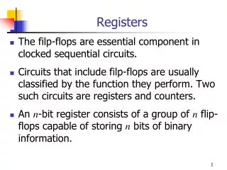
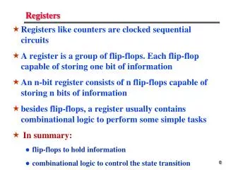
Registers. Registers like counters are clocked sequential circuits A register is a group of flip-flops. Each flip-flop capable of storing one bit of information An n-bit register consists of n flip-flops capable of storing n bits of information

E N D
Registers Registers like counters are clocked sequential circuits A register is a group of flip-flops. Each flip-flop capable of storing one bit of information An n-bit register consists of n flip-flops capable of storing n bits of information besides flip-flops, a register usually contains combinational logic to perform some simple tasks In summary: • flip-flops to hold information • combinational logic to control the state transition
I0 A0 D Q R R R R I1 A1 D Q I2 A2 Reset D Q I3 A3 D Q CLK Registers • Group of D Flip-Flops • Synchronized (Single Clock) • Store Data
I0 A0 D Q CLK I3 R R R R I1 A1 I2 D Q I1 I0 I2 A2 Reset D Q I3 A3 D Q CLK Registers A3 A2 A1 A0 Note: New data has to go in with every clock
REGISTER Q7 Q6 Q5 Q4 Q3 Q2 Q1 Q0 D7 D6 D5 D4 D3 D2 D1 D0 LD Registers with Parallel Load • Control Loading the Register with New Data
I0 A0 D Q I1 A1 D Q ClK I2 A2 D Q Load CLK I3 A3 D Q Load CLK Registers with Parallel Load • Should we block the “Clock” to keep the “Data”? Delays the Clock
Registers with Parallel Load A0 I0 A1 I1 A2 I2 A3 I3
I0 I1 MUX I0 I1 MUX I0 I1 MUX I0 I1 MUX Y Y Y Y S S S S Registers with Parallel Load • Circulate the “old data” A0 D Q I0 A1 D Q I1 A2 D Q I2 D Q A3 I3 Load CLK
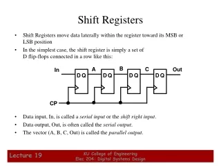
SI SO D D D D Q Q Q Q CLK Shift Registers • 4-Bit Shift Register SerialInput SerialOutput
D D D D Q Q Q Q CLK SI Shift Registers Q3 Q2 Q1 Q0 SI SO CLK Q3 Q2 Q1 Q0
I0 I0 B0 A0 D D Q Q R R R R R R R R I1 I1 B1 A1 D D Q Q I2 I2 B2 A2 Reset Reset D D Q Q I3 I3 B3 A3 D D Q Q CLK CLK Parallel transfere
Clock ShiftControl D D D D Q Q Q Q Clock ShiftControl CLK Serial Transfer Q3 Q2 Q1 Q0 SI SO SI SO SI Shift Register A Shift Register B CLK CLK
Shift Register A Shift Register B Serial Addition SI ShiftControl FA x y z S C SI CLK Q D CLR Clear
Shift Register A Shift Register B Serial Addition SI ShiftControl 1 0 FA x y z 1 S C SI 1 CLK 0 Q D CLR Clear
Shift Register A Shift Register B Serial Addition SI ShiftControl 1 0 FA x y z 0 S C SI 1 CLK 1 Q D CLR Clear
Shift Register A Shift Register B Serial Addition SI ShiftControl 0 1 FA x y z 0 S C SI 0 CLK 1 Q D CLR Clear
Shift Register A Shift Register B Serial Addition SI ShiftControl 0 1 FA x y z 1 S C SI 0 CLK 0 Q D CLR Clear
Shift Register A Shift Register B Serial Addition SI ShiftControl 0 0 FA x y z 0 S C SI 0 CLK 0 Q D CLR Clear
D D D D Q Q Q Q Universal Shift Register • Parallel-in Parallel-out (PI/PO) • Serial-in Serial-out (SI/SO) • Serial-in Parallel-out(SI/PO) • Parallel-in Serial-out(PI/SO)
Q3 Q2 Q1 Q0 Q Q Q Q CLR D D D D CLK PI/PO SI for SL SI for SR p3 P2 P1 P0
D D D D Q Q Q Q SI/SO Q3 Q2 Q1 Q0 SI for shift right SO CLK
CLR Universal Shift Register Q3 Q2 Q1 Q0 S1 S0 USR SRin SLin D3 D2 D1 D0
Q3 Q2 Q1 Q0 Q Q Q Q CLR D D D D CLK S1S0 Y MUX I3I2I1I0 Universal Shift Register S1S0 I2 I1 SI for SL SI for SR D3 D2 D1 D0
Q3 Q2 Q1 Q0 1 1 1 1 CLK T T T T Q Q Q Q CLR CLR CLR CLR CLR CLK Ripple Counters • Ripple ↔ Asynchronous Q0 Q1 Q2 Q3
Q Q Q Q D D D D Q Q Q Q CLK Q0 Q1 Q2 Q3 Ripple Counters Q3 Q2 Q1 Q0 CLK 0 1 2 3 4 5 6 7 8 9
0010 0011 0100 0000 0001 0111 1001 1000 0110 0101 Q3 Q2 Q1 Q0 1 1 Q Q Q Q J J J J CLK Q Q Q Q K K K K 1 1 1 1 BCD Ripple Counter
Decades Counter Q3 Q2 Q1 Q0 Q3 Q2 Q1 Q0 Q3 Q2 Q1 Q0 BCDCounter BCDCounter BCDCounter Count (CLK) 100’s Digit 10’s Digit 1’s Digit
Q Q Q Q J J J J Q Q Q Q K K K K Synchronous Binary Counter Q3 Q2 Q1 Q0 Enable To Next Stage CLK
Q Q Q Q T T T T Q Q Q Q Up-Down Binary Counter Q3 Q2 Q1 Q0 CLK Up Down
BCD Counter 0 0 0 0 0 1 1 1 1 0000 / 0 0001 / 0 0010 / 0 0011 / 0 0100 / 0 1 1 1001 / 1 1000 / 0 0111 / 0 0110 / 0 0101 / 0 1 1 1 1 0 0 0 0 0 Q3 Q2 Q1 Q0 y E
Binary Counter with Parallel Load I3 Q3 I2 Q2 I1 Q1 I0 Q0 LD Count CLR Usually Asynchronous Clear
BCD Counter Example 1 LD LD Q3 Q3 I3 I3 0 0 A3 A3 0 0 I2 I2 Q2 Q2 A2 A2 Q1 Q1 I1 I1 0 0 A1 A1 0 0 I0 I0 Q0 Q0 A0 A0 Count Count Count Count CLR CLR CLK CLK 1
CLK T3 T2 T1 T0 T0 2-to-4 Decoder T1 T2 2-bit counter T3 Ring Counter 1000 0100 0010 0001
Johnson Counter 0000 1000 1100 1110 0001 0011 0111 1111 A k-bit ring counter can generate k distinguishable states The number of states can be doubled if the shift register is connected as a switch-tail ring counter
Q Q Q Q D D D D Q1 Q3 Q2 Q0 Q Q Q Q CLK Johnson Counter
Johnson Counter Not self correcting
Johnson Counter Correction: make DC=(A+C)B Unused sates go towards used states
Homework • Mano • Chapter 6 • 6-2 • 6-3 • 6-4 • 6-13 • 6-14 • 6-16 • 6-18