Download
1 / 25
290 likes | 514 Views
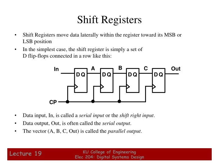
Shift Registers. Shift Registers move data laterally within the register toward its MSB or LSB position In the simplest case, the shift register is simply a set of D flip-flops connected in a row like this: Data input, In, is called a serial input or the shift right input .

E N D
Shift Registers • Shift Registers move data laterally within the register toward its MSB or LSB position • In the simplest case, the shift register is simply a set of D flip-flops connected in a row like this: • Data input, In, is called a serial input or the shift right input. • Data output, Out, is often called the serial output. • The vector (A, B, C, Out) is called the parallel output. KU College of Engineering Elec 204: Digital Systems Design
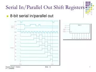
CP In A B C Out T0 0 ? ? ? ? T1 1 0 ? ? ? T2 1 1 0 ? ? T3 0 1 1 0 ? T4 1 T5 1 T6 1 Shift Registers (continued) B A C Out In D Q D Q D Q D Q • The behavior of theserial shift registeris given in the listingon the lower right • T0 is the register state just before the first clockpulse occurs • T1 is after thefirst pulse andbefore the second. • Initially unknownstates are denoted by “?” • Complete the last threerows of the table Clock CP KU College of Engineering Elec 204: Digital Systems Design
Time and Shift Controlled Structure KU College of Engineering Elec 204: Digital Systems Design
Serial Addition • Serial operations: slower, smaller • Parallel operations: faster but requires more chip area • Perform: A+B A KU College of Engineering Elec 204: Digital Systems Design
Serial Adder Load/Right Shift Registers Serial • The circuit shown uses two shiftregisters for operands A(3:0)and B(3:0). • A full adder, and one moreflip flop (for the carry) is usedto compute the sum. • The result is stored in theA register and the finalcarry in the flip-flop • With the operands and theresult in shift registers, a tree of full adders can beused to add a large number of operands. Used as a common digital signal processing technique. In A FA B A3 A2 A1 A0 Sum Parallel Load Cin Serial Cout In B3 B2 B1 B0 Parallel Load Q D CP (Clock and Load/Shift Control not shown) KU College of Engineering Elec 204: Digital Systems Design
Parallel Load Shift Registers DA DB A B • By adding a muxbetween each shift registerstage, data can beshifted or loaded • If SHIFT is low,A and B arereplaced by the data on DA and DB lines, else data shifts right on each clock. • By adding more bits, we can make n-bit parallel load shift registers. • A parallel load shift register with an added “hold” operation that stores data unchanged is given in Figure 7-10 of the text. D D IN Q Q SHIFT CP KU College of Engineering Elec 204: Digital Systems Design
Shift Registers with Additional Functions • By placing a 4-input multiplexer in front of each D flip-flop in a shift register, we can implement a circuitwith shifts right, shifts left, parallel load, hold. • Shift registers can also be designed to shift more than a single bit position right or left • Shift register can be designed to shift a variable number of bit positions specified by a variable called a shift amount. KU College of Engineering Elec 204: Digital Systems Design
Counters • Counters are sequential circuits which "count" through a specific state sequence. They can count up, count down, or count through other fixed sequences. Two distinct types are in common usage: • Ripple Counters • Clock is connected to the flip-flop clock input on the LSB bit flip-flop • For all other bits, a flip-flop output is connected to the clock input, thus circuit is not truly synchronous • Output change is delayed more for each bit toward the MSB. • Resurgent because of low power consumption • Synchronous Counters • Clock is directly connected to the flip-flop clock inputs • Logic is used to implement the desired state sequencing KU College of Engineering Elec 204: Digital Systems Design
A D Clock CR D B CR Reset CP A B 0 1 0 1 2 3 Ripple Counter • How does it work? • When there is a positive edge on the clock inputof A, A complements • The clock input for flip-flop B is the complementedoutput of flip-flop A • When flip A changesfrom 1 to 0, there is apositive edge on theclock input of Bcausing B tocomplement KU College of Engineering Elec 204: Digital Systems Design
CP A B 0 1 0 1 2 3 (0,1), (1,0), (1,1), (0,0), (0,1), … Ripple Counter (continued) • The arrows show thecause-effect relation-ship from the priorslide => • The correspondingsequence of states =>(B,A) = (0,0), • Each additional bit, C, D, …behaves like bit B, changing half as frequently as the bit before it. • For 3 bits: (C,B,A) = (0,0,0), (0,0,1), (0,1,0), (0,1,1),(1,0,0), (1,0,1), (1,1,0), (1,1,1), (0,0,0), … KU College of Engineering Elec 204: Digital Systems Design
Ripple Counter (continued) • These circuits are called ripple counters because each edge sensitive transition (positive in the example) causes a change in the next flip-flop’s state. • The changes “ripple” upward through the chain of flip-flops, i. e., each transition occurs after a clock-to-output delay from the stage before. • To see this effect in detail look at the waveforms on the next slide. KU College of Engineering Elec 204: Digital Systems Design
tPHL CP tPHL A tpHL B C Ripple Counter (continued) • Starting with C = B = A = 1, equivalent to (C,B,A) = 7 base 10, the next clock increments the count to (C,B,A) = 0 base 10. In fine timing detail: • The clock to output delaytPHL causes an increasingdelay from clock edge foreach stage transition. • Thus, the count “ripples”from least to mostsignificant bit. • For n bits, total worst casedelay is n tPHL. KU College of Engineering Elec 204: Digital Systems Design
Synchronous Counters • To eliminate the "ripple" effects, use a common clock for each flip-flop and a combinational circuit to generate the next state. • For an up-counter,use an incrementer => Incre-menter S3 D3 Q3 A3 Q2 S2 D2 A2 S1 Q1 D1 A1 S0 D0 Q0 A0 Clock KU College of Engineering Elec 204: Digital Systems Design
Incrementer Synchronous Counters (continued) • Internal details => • Internal Logic • XOR complements each bit • AND chain causes complementof a bit if all bits toward LSBfrom it equal 1 • Count Enable • Forces all outputs of ANDchain to 0 to “hold” the state • Carry Out • Added as part of incrementer • Connect to Count Enable ofadditional 4-bit counters toform larger counters KU College of Engineering Elec 204: Digital Systems Design
Synchronous Counters (continued) • Carry chain • series of AND gates through which thecarry “ripples” • Yields long path delays • Called serial gating • Replace AND carry chain with ANDs =>in parallel • Reduces path delays • Called parallel gating • Like carry lookahead • Lookahead can be used on COsand ENs to prevent long paths inlarge counters • Symbol for Synchronous Counter KU College of Engineering Elec 204: Digital Systems Design
Other Counters • See text for: • Down Counter - counts downward instead of upward • Up-Down Counter - counts up or down depending on value a control input such as Up/Down • Parallel Load Counter - Has parallel load of values available depending on control input such as Load • Divide-by-n (Modulo n) Counter • Count is remainder of division by n which n may not be a power of 2 or • Count is arbitrary sequence of n states specifically designed state-by-state • Includes modulo 10 which is the BCD counter KU College of Engineering Elec 204: Digital Systems Design
Load Count Q D D 0 0 C Q D D 1 1 C Q D D 2 2 C Q D D 3 3 C Carry Output CO Clock Counter with Parallel Load • Add path for input data • enabled for Load = 1 • Add logic to: • disable count logic for Load = 1 • disable feedback from outputsfor Load = 1 • enable count logic for Load = 0and Count = 1 • The resulting function table: KU College of Engineering Elec 204: Digital Systems Design
Current State Next State Q8 Q4 Q2 Q1 Q8 Q4 Q2 Q1 0 0 0 0 0 0 0 1 0 0 0 1 0 0 1 0 0 0 1 0 0 0 1 1 0 0 1 1 0 1 0 0 0 1 0 0 0 1 0 1 0 1 0 1 0 1 1 0 0 1 1 0 0 1 1 1 0 1 1 1 1 0 0 0 1 0 0 0 1 0 0 1 1 0 0 1 0 0 0 0 Design Example: Synchronous BCD • Use the sequential logic model to design a synchronous BCD counter with D flip-flops • State Table => • Input combinations1010 through 1111are don’t cares KU College of Engineering Elec 204: Digital Systems Design
Synchronous BCD (continued) • Use K-Maps to two-level optimize the next state equations and manipulate into forms containing XOR gates: D1 = Q1 D2 = Q2 + Q1Q8 D4 = Q4 + Q1Q2 D8 = Q8 + (Q1Q8 + Q1Q2Q4) • The logic diagram can be draw from these equations • An asynchronous or synchronous reset should be added • What happens if the counter is perturbed by a power disturbance or other interference and it enters a state other than 0000 through 1001? KU College of Engineering Elec 204: Digital Systems Design
0 9 1 14 2 8 15 12 13 3 7 11 10 6 4 5 Synchronous BCD (continued) • Find the actual values of the six next states for the don’t care combinations from the equations • Find the overall state diagram to assess behavior for the don’t care states (states in decimal) KU College of Engineering Elec 204: Digital Systems Design
Synchronous BCD (continued) • For the BCD counter design, if an invalid state is entered, return to a valid state occurs within two clock cycles • Is this adequate? If not: • Is a signal needed that indicates that an invalid state has been entered? What is the equation for such a signal? • Does the design need to be modified to return from an invalid state to a valid state in one clock cycle? • Does the design need to be modified to return from a invalid state to a specific state (such as 0)? • The action to be taken depends on: • the application of the circuit • design group policy • See pages 278 - 279 of the text. KU College of Engineering Elec 204: Digital Systems Design
Counting Modulo N • The following techniques use an n-bit binary counter with asynchronous or synchronous clear and/or parallel load: • Detect a terminal count of N in a Modulo-N count sequence to asynchronously Clear the count to 0 or asynchronously Load in value 0 (These lead to counts which are present for only a very short time and can fail to work for some timing conditions!) • Detect a terminal count of N - 1 in a Modulo-N count sequence to Clear the count synchronously to 0 • Detect a terminal count of N - 1 in a Modulo-N count sequence to synchronously Load in value 0 • Detect a terminal count and use Load to preset a count of the terminal count value minus (N - 1) • Alternatively, custom design a modulo N counter as done for BCD KU College of Engineering Elec 204: Digital Systems Design
Counting Modulo 7: Detect 7 and Asynchronously Clear Q3 D3 • A synchronous 4-bit binary counterwith an asynchronous Clear isused to make a Modulo7 counter. • Use the Clear feature todetect the count 7 andclear the count to 0. Thisgives a count of 0, 1, 2, 3, 4,5, 6, 7(short)0, 1, 2, 3, 4, 5,6, 7(short)0, etc. • DON’T DO THIS! Referred to as a “suicide” counter! (Count “7” is “killed,” but the designer’s job may be dead as well!) Q2 D2 Q1 D1 Q0 D0 Clock CP 0 LOAD CLEAR KU College of Engineering Elec 204: Digital Systems Design
0 Q3 D3 0 Q2 D2 0 Q1 D1 0 Q0 D0 Clock CP LOAD Reset CLEAR Counting Modulo 7: Synchronously Load on Terminal Count of 6 • A synchronous 4-bit binarycounter with a synchronousload and an asynchronousclear is used to make a Modulo 7 counter • Use the Load feature todetect the count "6" andload in "zero". This givesa count of 0, 1, 2, 3, 4, 5, 6,0, 1, 2, 3, 4, 5, 6, 0, ... • Using don’t cares for statesabove 0110, detection of 6 can be done with Load = Q4 Q2 KU College of Engineering Elec 204: Digital Systems Design
Counting Modulo 6: Synchronously Preset 9 on Reset and Load 9 on Terminal Count 14 1 Q3 D3 • A synchronous, 4-bit binarycounter with a synchronousLoad is to be used to make aModulo 6 counter. • Use the Load feature topreset the count to 9 onReset and detection ofcount 14. • This gives a count of 9, 10, 11, 12, 13, 14, 9, 10, 11, 12, 13, 14, 9, … • If the terminal count is 15 detection is usually built in as Carry Out (CO) 0 Q2 D2 0 Q1 D1 1 Q0 D0 Clock CP Reset LOAD CLEAR 1 KU College of Engineering Elec 204: Digital Systems Design