Download
1 / 58
580 likes | 586 Views
Chapter 5: Datapath and Control. CS 447 Jason Bakos. Review of Digital Logic. Review AND, OR, NOT, and XOR gates Review negative-logic (inverted) inputs and outputs NAND, NOR, XNOR Sum-of-products with NAND gates Product-of-sums with NOR gates “Double-bubble” cancellation DeMorgan’s Law

E N D
Chapter 5: Datapath and Control CS 447 Jason Bakos
Review of Digital Logic • Review AND, OR, NOT, and XOR gates • Review negative-logic (inverted) inputs and outputs • NAND, NOR, XNOR • Sum-of-products with NAND gates • Product-of-sums with NOR gates • “Double-bubble” cancellation • DeMorgan’s Law • Completeness of NAND and NOR gates • Review of muxes and decoders • Boolean algebra equations vs. digital logic gate schematics • Review of truth tables • Product-of-sums
Review of Digital Logic • Logic minimization • Boolean algebra • Identity Law • A+0=A and A*1=A • Zero and One Laws • A+1=1 and A*0=0 • Inverse Laws • A + (not A)=1 and A*(not A)=0 • Commutative Laws • A+B=B+A and A*B=B*A • Associative Laws • A+(B+C)=(A+B)+C and A*(B*C)=(A*B)*C • Distributive Laws • A*(B+C)=AB+AC and A+(B*C)=(A+B)*(A+C) • DeMorgan’s Law • not (A+B)=(not A)*(not B) and not(A*B)=(not A)+(not B)
Review of Digital Logic • Review Karnaugh Map logic minimization • mux2 example • Review “don’t care” logic minimization • mux2 example • Review Boolean algebra logic minimization • mux2 example
Memory Devices • Consider cross-coupled NOR gates • This is the most simple memory device, called an SR-flip-flop Let’s eliminate the S input and provide a clock input In this configuration, the clock acts as an “enable” and is a level sensitive clock
Memory Devices • Clocked memory devices are divided into two categories: • Latches are level-sensitive devices where the output samples the input the entire time the clock signal is high: • Latches are “transparent”, they are open whenever the clock is asserted • Flip-flips only sample the input on the rising or falling edge of the clock • We only want state changes on one of the edges of the clock
Memory Devices • Here’s a master-slave approach to designing a falling-edge triggered FF • Here’s a timing diagram for this device
Memory Devices • Flip flops, depending on their design and technology, have set-up and hold times • Set-up time is the amount of time the input signal (D) must be stable prior to the clock edge that samples it • Hold time is the amount of time the input signal (D) must be stable after the clock edge
Memory Devices • For the master-slave design, the set-up time was very long, which is why we need a better design • We won’t get into other ways to design edge-triggered flip-flips, but there are many with varying numbers of gates • Usually the classic SR-latch acts as a building block for such devices • Flip-flips also have asynchronous sets/resets and sometimes enables • Some textbooks refer to the last design as a “pulse”-trigger flip-flip, since the input must be stable for the entire clock pulse
Finite State Machines (FSM) • So far we’ve mainly did circuit design with combinational logic systems • Combinational logic circuits have an output that is some function of the inputs • Next we’re going to start using sequential systems • Sequential circuits have an output that is some function of the inputs and its input history • The first example of these are state machines
Finite State Machines (FSM) • State machines can be either synchronous or asynchronous • Synchronous state machines only change state with a clock event (edge) • Asynchronous state machines do not have this restriction • We’ll start by building a synchronous state machine • We’ll assume we have access to good positive edge triggered D flip-flip cells
Finite State Machines • Here’s two different representations of the FSM in digital logic:
Finite State Machines • There are two different ways of designing state machines: Mealy and Moore • In all state machines, the next state (which will be the current state after the next clock edge) is computed as a combinational function of the current state and the inputs • The outputs, on the other hand, are computed either as a function of the current state or as a function of the current state AND the inputs (hence Moore vs. Mealy) • Note: Moore is less, because Moore machines are restricted to synchronous outputs (outputs that only change on a clock edge) Mealy machines do not have this restriction
Finite State Machines • In order to build a state machine, we must first have our input signals and output signals • Then we start adding states and transitions • For a Mealy machine, the outputs will be on the transitions • For a Moore machine, the outputs will be in the states
Finite State Machines • Next, we need to encode state values for each of our states • Try to minimize bit changes on state transitions • Recall: We’ll need lg n flip-flops if we have n states • Then, use Karnaugh maps to minimize our next-state and output logic • Note: we could use a state machine table (truth table)
Finite State Machine Examples • First, let’s tackle an example • 3 bit counter • Outputs: 3 counter bits (no inputs) • Here’s another example • Let’s design a combination lock with 2-bit combination inputs and an enter key • The output will be an “unlock” signal • Next, let’s do a Coke machine example (where a coke is 35 cents) • Inputs: quarter, dime, nickel • Output: release_coke
Registers • A register is simply an array of D-flip-flops (8-bit, 32-bit, etc.) • The important distinction between flip-flips and registers is that it is VERY important for registers to have enable inputs
Wide Multiplexors • Wide multiplexors (not an official name) are simply an array of single muxes • For example, if we want a 32 bit 4-to-1 mux, we need to array 32 4-to-1 muxes • Using state machine controllers, registers, and muxes, we can very easily implement control for a digital system
Example: Checksummer • You are to design a device that accepts a data packet comprised of a series of 8-bit words. The packet format is the following: • Each 8-bit word is valid on the falling edge of each clock. The synch. characters signal the beginning of a new packet. Synch. character 1 is “00110011” and synch. character 2 is “11001100”. The length field specifies how many words are contained in the data portion of the packet. The data payload is the actual data payload of the packet (which can be anything). Your device will keep a running modulo 256 sum of these data words and compare that value to the value of the checksum field at the end of the packet.
Example: Checksummer • Your device has the following input signals: • Clock – clock input • DataIn – 8-bit bus that puts a new character out on every falling edge of the clock • Reset – active-high reset • The device will have the following output signals: • ChecksumError – this signal will be asserted for one clock cycle following the data input if there is a checksum error in the data packet. I must be valid on the rising edge that defines the end of the checksum word. • DataValid – this signal goes high at the on the rising edge that defines the beginning of the payload and goes low on the rising edge the defines the beginning of the checksum word.
Example: Checksummer • First, what type of components do we need for this device? • How do we design the state machine control? • There’s too many signals to actually implement the controller on the board • How do we interconnect this device?
Chapter 5: Datapath and Control(Part 2) CS 447 Jason Bakos
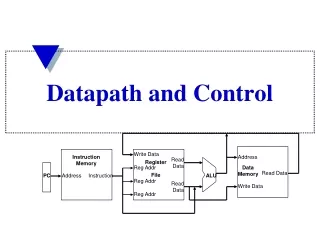
Building a Datapath • Which components do we need for the A/L, load, and branch classes of MIPS instructions? • First, we need a memory to hold our instructions • Assume it has an address input, data output, and a MemRead and MemWrite control signals • A Program Counter (PC) register to hold the address of the next instruction • Typical register (clk, en, rst, D, and Q) • ALU (the one we built in Chap. 4) • A, B, ALUOp, and Out • Register file • Dual-port (ReadAddr1, ReadAddr2, WriteReg, WriteData, RegWrite, ReadData1, ReadData2) • Instruction Register • Like the PC, but holds the current instruction word
Datapaths • Assuming our instruction is already fetched, using our components we need to build datapaths for the following: • PC=PC+4 • Executing A/L R-type instruction and writing back result • Executing load/store effective address calculation • We need a sign extender for this • Computing a branch target address and determining whether or not a branch should be taken (for beq) • We need a sign extender and a 2-bit shifter for this
Datapaths PC+4 datapath R-type A/L datapath
Datapaths Load/Store Datapath
Datapaths Branch (beq) Datapath
Simple CPU Implementation • We want to implement the simplest possible implementation of our MIPS subset of instructions • lw/sw • beq • add, sub, and, or, and slt
Combining Datapaths • Let’s combine the datapaths that we looked at into a single datapath • Let’s assume that we want to execute all our instructions in a single clock cycle • This means that we can only use each datapath component once per instruction • We need a separate instruction and data memory • We may need to duplicate some components (but we can share components across different instruction types) • We need multiplexors for this
Integrated Datapaths • Here we combine all our datapaths • We also add our fetch hardware • Next we’ll need a control unit to assert the control signals
Control Signals • Recall the ALU control table… • Let’s create a small control “lookup table” for the ALU...
Control Signals • Note that ALUOp will come from the main control unit
Designing the Main Control Unit • First, let’s take a look at all our current control signals and their effect...
R-type Control • For an R-type instruction, let’s decide what needs to be done (note this is done in parallel) • Fetch instruction and increment PC by 4 • Read two registers • ALU does computation • Result is written back to register file
Load/Store Control • Let’s decide what needs to be done for a lw instruction • Fetch/increment PC • Read base register from reg. file • ALU computes effective address (base+offset) • Data from memory is written back to register file
Branch-on-Equal Control • Finally, let’s decide what needs to be done in order to perform the beq instruction • Fetch/increment PC • Read two registers • ALU subtracts • ALU computes effective branch target (PC+offset*4) • Zero result from ALU decides if we should write the new value to the PC
Control • Next time we’ll find out why a single-cycle CPU like this is not practical • We need a FSM to handle control in order to reuse components during a single instruction execution
Chapter 5: Datapath and Control(Part 3) CS 447 Jason Bakos
Single-Cycle CPU • CPI of the single cycle CPU from the last lecture had a CPI of 1 • Clock cycle is determined by the longest possible path in the machine • loads are the worst – they use 5 functional units in series • Performance, utilization, and efficiency are not going to be good, because most instructions don’t need such a long clock cycle • A variable-speed clock could be used to solve this problem, but hinders parallelism • Pipelining overlaps instruction executions
Multicycle Implementation • Break instructions into steps, where each step requires one clock cycle • We want to reuse functional units within an instruction instead of just across instructions • Reduces hardware • Use single memory for instructions and data • Single ALU instead of one ALU and two adders • Add registers to functional units to hold intermediate results (state data) for future cycles • Use within instruction executions • Register file and memory hold state data to be used across instruction executions • These are programmer-visible • We will need a FSM to control CPU
Registers • Locations of registers is determined by the following: • What combinatorial units will fit in one clock cycles • Assume memory access, regfile access (two reads or one write), or ALU operation • Any data needed by these operations must be stored in a temporary register • Instruction Register, Memory Data Register, A, B, and ALUOut registers added to design • All these except IR only need to hold data between two adjacent clock cycles • What data are needed in later cycles implementing the instruction
Multiplexors • Need to add extra multiplexors (or expand existing muxes) to facilitate the reuse of the ALU within instructions • Add mux to first ALU input • Expand mux to second ALU input
Breaking Instruction Execution into Clock Cycles • Goal is to balance the latency of the operations performed during each clock cycle • At most one of the following can occur in series: • One ALU operation • One register file access (or multiple in parallel) • One memory access (this is a joke, but we’ll accept this for now)
Execution Stages • In order to clearly define the CPU operation for each step in the operation, we’ll use RTL (register transfer language) • Architecture research has defined 5 standard phases of instruction execution • Instruction fetch • Decode • Fetch register values from register file • Execute • Perform arithmetic/logic operation • Memory • Load/Store memory • Write back • Write register result back to register file
Execution Stages • Fetch • IR=Memory[PC] • PC=PC+4 • Decode • A=Reg[IR[25..21]] • B=Reg[IR[20..16]] • ALUOut=PC+(sign_extend(IR[15..0]) << 2
Execution Stages • Execute • Memory access • ALUOut=A+sign_extend(IR[15..0]) • R-type • ALUOut=A op B • Branch (beq) • if (A==B) PC=ALUOut • PC=PC[31..28] || (IR[25..0]<<2)