Download
1 / 25
280 likes | 375 Views
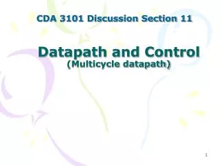
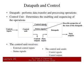
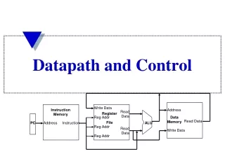
Write Data. Instruction Memory. Address. Read Data. Register File. Reg Addr. Data Memory. Read Data. PC. Address. Instruction. ALU. Reg Addr. Read Data. Write Data. Reg Addr. Datapath and Control. Five Instruction Steps.

E N D
Write Data Instruction Memory Address Read Data Register File Reg Addr Data Memory Read Data PC Address Instruction ALU Reg Addr Read Data Write Data Reg Addr Datapath and Control
Five Instruction Steps • The control architecture can be treated as a Moore State Machine, with output depending only on the current state. States change at every clock cycle. • Instructions need different number of cycles (3-5) depending on the number of steps they have. • Some steps are common for all instructions. • Example - Instruction Fetch step • Also common is Instruction Decode and Register Fetch step • R-type Instruction Execution, Memory Read/Write Address Computation, Branch Completion, or Jump Completion are different • Memory Read Access, Memory Write Completion or R-type Instruction Completion • Memory Read Completion (Write Back)
Step 1: Instruction Fetch • Use PC to get instruction from the memory and put it in the Instruction Register MemoryRead=1, IRWrite=1, • Increment the PC by 4 and put the result back in the PC IorD=0 (to select PC), ALUSrcA=0, ALUSrcB=01, ALUOp=00 (add), PCWrite=1 • Can be described succinctly using RTL "Register-Transfer Language“ IR = Memory[PC]; PC = PC + 4;
PCWrite MemRead ALUSrcB IRWrite MDR Datapath Activity During Instruction Fetch PCWriteCond PCSource IorD ALUOp Control MemWrite ALUSrcA MemtoReg RegWrite RegDst PC[31-28] Instr[31-26] Shift left 2 28 Instr[25-0] 2 0 1 Address Memory 0 PC 0 Read Addr 1 A Read Data 1 IR Register File 1 1 zero Read Addr 2 Read Data (Instr. or Data) 0 ALUout ALU Write Addr Write Data 1 Read Data 2 B 0 1 Write Data 4 1 0 2 Instr[15-0] Sign Extend Shift left 2 3 32 ALU control Instr[5-0]
Fetch Control Signals Settings State 0 IorD=0 MemRead;IRWrite ALUSrcA=0 ALUsrcB=01 PCSource,ALUOp=00 PCWrite Instr Fetch Start
Step 2: Instruction Decode and Register Fetch • Don’t know what the instruction is yet, so can only • Read registers rs and rt in case we need them • Compute the branch address in case the instruction is a branch ALUSrcB=11, ALUOp=00 (add), ALUSrcA=0 (select PC) • RTL: A = Reg[IR[25-21]];B = Reg[IR[20-16]];ALUOut = PC +(sign-extend(IR[15-0])<< 2); • We aren't setting any control lines based on the instruction (since we are busy "decoding" it in our control logic)
MDR Datapath Activity During Instruction Decode PCWriteCond PCWrite PCSource IorD ALUOp MemRead Control ALUSrcB MemWrite ALUSrcA MemtoReg RegWrite IRWrite RegDst PC[31-28] Instr[31-26] Shift left 2 28 Instr[25-0] 2 0 1 Address Memory 0 PC 0 Read Addr 1 A Read Data 1 IR Register File 1 1 zero Read Addr 2 Read Data (Instr. or Data) 0 ALUout ALU Write Addr Write Data 1 Read Data 2 B 0 1 Write Data 4 1 0 2 Instr[15-0] Sign Extend Shift left 2 3 32 ALU control Instr[5-0]
Decode IorD=0 MemRead;IRWrite ALUSrcA=0 ALUsrcB=01 PCSource,ALUOp=00 PCWrite Instr Fetch Unless otherwise assigned PCWrite,IRWrite, MemWrite,RegWrite=0 others=X Start Decode Control Signals Settings ALUSrcA=0 ALUsrcB=11 ALUOp=00
Step 3 (instruction dependent) • ALU is performing one of four functions, based on instruction type • Memory reference (lw and sw): ALUop=00, ALUSrcB=10, ALUSrcA=1 ALUOut = A + sign-extend(IR[15-0]); • R-type: ALUop=10 (use function field), ALUSrcA=1, ALUScrB=00 ALUOut = A op B;
Step 3 (instruction dependent) • Branch: ALUSrcB=00, ALUSrcA=1, ALUop=01 (force subtraction), PCSource=01 (use ALUout), PCwritecond=1 (in case zero=1) if (A==B) PC = ALUOut; • Jump: PCWrite=1, PCsource=10 PC = PC[31-28] || (IR[25-0] << 2);
MDR Datapath Activity During Instruction Execute PCWriteCond PCWrite PCSource IorD ALUOp MemRead Control ALUSrcB MemWrite ALUSrcA MemtoReg RegWrite IRWrite RegDst PC[31-28] Instr[31-26] Shift left 2 28 Instr[25-0] 2 0 1 Address Memory 0 PC 0 Read Addr 1 A Read Data 1 IR Register File 1 1 zero Read Addr 2 Read Data (Instr. or Data) 0 ALUout ALU Write Addr Write Data 1 Read Data 2 B 0 1 Write Data 4 1 0 2 Instr[15-0] Sign Extend Shift left 2 3 32 ALU control Instr[5-0]
Decode IorD=0 MemRead;IRWrite ALUSrcA=0 ALUsrcB=01 PCSource,ALUOp=00 PCWrite Instr Fetch Unless otherwise assigned PCWrite,IRWrite, MemWrite,RegWrite=0 others=X ALUSrcA=0 ALUSrcB=11 ALUOp=00 PCWriteCond=0 Start (Op = R-type) (Op = beq) (Op = lw or sw) (Op = j) ALUSrcA=1 ALUSrcB=10 ALUOp=00 PCWriteCond=0 ALUSrcA=1 ALUSrcB=00 ALUOp=01 PCSource=01 PCWriteCond ALUSrcA=1 ALUSrcB=00 ALUOp=10 PCWriteCond=0 PCSource=10 PCWrite Execute Control Signals Settings Execute
Step 4 (instruction dependent) • Memory reference: MemoryRead=1, IorD=1 MDR = Memory[ALUOut]; -- lwor MemoryWrite=1, IorD=1 Memory[ALUOut] = B;-- sw • R-type instruction completion RegDst=1, RegWrite=1, MemtoReg=0 Reg[IR[15-11]] = ALUOut; • Remember, the register write actually takes place at the end of the cycle on the clock edge
MDR Datapath Activity During Memory Access PCWriteCond PCWrite PCSource IorD ALUOp MemRead Control ALUSrcB MemWrite ALUSrcA MemtoReg RegWrite IRWrite RegDst PC[31-28] Instr[31-26] Shift left 2 28 Instr[25-0] 2 0 1 Address Memory 0 PC 0 Read Addr 1 A Read Data 1 IR Register File 1 1 zero Read Addr 2 Read Data (Instr. or Data) 0 ALUout ALU Write Addr Write Data 1 Read Data 2 B 0 1 Write Data 4 1 0 2 Instr[15-0] Sign Extend Shift left 2 3 32 ALU control Instr[5-0]
RegDst=1 RegWrite MemtoReg=0 PCWriteCond=0 MemRead IorD=1 PCWriteCond=0 MemWrite IorD=1 PCWriteCond=0 Memory Access Control Signals Settings Decode IorD=0 MemRead;IRWrite ALUSrcA=0 ALUsrcB=01 PCSource,ALUOp=00 PCWrite Instr Fetch Unless otherwise assigned PCWrite,IRWrite, MemWrite,RegWrite=0 others=X ALUSrcA=0 ALUSrcB=11 ALUOp=00 PCWriteCond=0 Start (Op = R-type) (Op = beq) (Op = lw or sw) (Op = j) ALUSrcA=1 ALUSrcB=10 ALUOp=00 PCWriteCond=0 ALUSrcA=1 ALUSrcB=00 ALUOp=01 PCSource=01 PCWriteCond ALUSrcA=1 ALUSrcB=00 ALUOp=10 PCWriteCond=0 PCSource=10 PCWrite Execute (Op = lw) (Op = sw) Memory Access
Step 5: Memory Read Completion (Write Back) • All we have left is the write back into the register file the data just read from memory for lw instruction RegDst=0, RegWrite=1, MemtoReg=1 Reg[IR[20-16]]= MDR;
MDR Datapath Activity During Write Back PCWriteCond PCWrite PCSource IorD ALUOp MemRead Control ALUSrcB MemWrite ALUSrcA MemtoReg RegWrite IRWrite RegDst PC[31-28] Instr[31-26] Shift left 2 28 Instr[25-0] 2 0 1 Address Memory 0 PC 0 Read Addr 1 A Read Data 1 IR Register File 1 1 zero Read Addr 2 Read Data (Instr. or Data) 0 ALUout ALU Write Addr Write Data 1 Read Data 2 B 0 1 Write Data 4 1 0 2 Instr[15-0] Sign Extend Shift left 2 3 32 ALU control Instr[5-0]
RegDst=0 RegWrite MemtoReg=1 Write Back Write Back Control Signals Settings Decode IorD=0 MemRead;IRWrite ALUSrcA=0 ALUsrcB=01 PCSource,ALUOp=00 PCWrite Instr Fetch Unless otherwise assigned PCWrite,IRWrite, MemWrite,RegWrite=0 others=X ALUSrcA=0 ALUSrcB=11 ALUOp=00 PCWriteCond=0 Start (Op = R-type) (Op = beq) (Op = lw or sw) (Op = j) ALUSrcA=1 ALUSrcB=10 ALUOp=00 PCWriteCond=0 ALUSrcA=1 ALUSrcB=00 ALUOp=01 PCSource=01 PCWriteCond ALUSrcA=1 ALUSrcB=00 ALUOp=10 PCWriteCond=0 PCSource=10 PCWrite Execute (Op = lw) (Op = sw) Memory Access RegDst=1 RegWrite MemtoReg=0 PCWriteCond=0 MemRead IorD=1 PCWriteCond=0 MemWrite IorD=1 PCWriteCond=0
Decode Instr Fetch IorD=0 MemRead;IRWrite ALUSrcA=0 ALUsrcB=01 PCSource,ALUOp=00 PCWrite ALUSrcA=0 ALUSrcB=11 ALUOp=00 PCWriteCond=0 RegDst=0 RegWrite=1 ALUOp=00 MemtoReg=0 Op = addi Op = addi State 12 State 1 State 0 Exercise 5.15 • Add addi to the classes of instructions supported - what influence on number of states of the machine? Instruction fetch and Instruction decode states are unchanged. ALUout = A+ sign-exte.(IR[15-0]) Completion Reg(IR[20-16])=ALUout
OP: addi RegDst=0 RegWrite=1 ALUOp=00 MemtoReg=0 State 12 Exercise 5.15 - Cont. • The finite state machine with the addition of the state to handle addi
Multi-cycle Control • Multi-cycle datapath control signals are not determined solely by the bits in the instruction • e.g., op code bits tell what operation the ALU should be doing, but not what instruction cycle is to be done next • We’ll use a finite state machine for control • a set of states (current state stored in State Register) • next state function (determined by current state and the input) • output function (determined by current state and the input)
PCWrite PCWriteCond IorD MemRead MemWrite IRWrite MemtoReg Combinational control logic PCSource Outputs ALUOp ALUSourceB ALUSourceA RegWrite RegDst Inputs Op5 Op4 Op3 Op2 Op1 Op0 Next State State Reg Inst[31-26] System Clock Finite State Machine Implementation • We’ll use a Moore machine (control signals based only on current state)