Download
1 / 23
230 likes | 442 Views
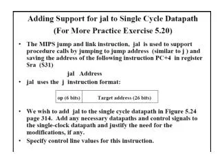
CDA 3101 Discussion Section 11. Datapath and Control (Multicycle datapath). Question 1. Show any necessary modifications in the multicycle datapath and control figures given on the next slides to support the following instruction. addm rd, rs, rt ; #rd = rs + Mem[rt]

E N D
CDA 3101 Discussion Section 11 Datapath and Control(Multicycle datapath)
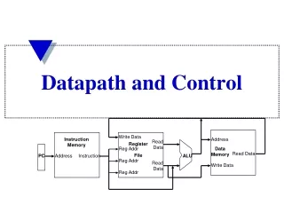
Question 1 Show any necessary modifications in the multicycle datapath and control figures given on the next slides to support the following instruction. addm rd, rs, rt ; #rd = rs + Mem[rt] This instruction is an R-format instruction. Make sure it does not break the other instructions (like add, sub, and, or, beq, lw, sw, j) which are supported by the datapath and control.
Question 1 We use the same datapath, but there are a few highly significant changes which must be made. 1. Instruction fetch: same 2. Instruction decode: - We will have to look at the funct field to determine that this instruction is addm. 3. Execution: - We have to get the second operand from memory before activating the ALU. 4. Instruction completion: Reg[IR[15-11]] = ALUOut.
Question 1 Instruction [5-0] 2 4
Question 1 (Op= R-type) and (Funct = addm) Memory Access MemRead IorD = 10 10 Execution 11 ALUSrcA = 1 ALUSrcB = 100 ALUOp = 00 (Assume that all IorD entries with 1 bit or ALUSrcB entries with 2 bits have a leading 0.)
Question 2 Consider the multi-cycle datapath in Fig. 5.28 and the FSM in Fig. 5.38 of the textbook. Say the datapath is executing the following instruction sequence: loop : add $t0,$t0,$t1 lw $t3, 0($t5) beq $t3,$t4,loop Assume the program counter is initially set to the ‘add’ instruction and the ‘add’ instruction is fetched in clock cycle 1. The add instruction will take 4 cycles, lw will take 5 cycles and beq will take 3 cycles to execute. Number these cycles 1, 2, 3, 4, 5, ….,12.
Question 2 (more) For each of these 12 cycles , provide the values for the various registers’ contents and the values of the control signals (listed below) that would exist in the circuit after all the “work” for that cycle has completed, right before the moment the rising edge of the next clock cycle occurs. Provide justification for each value you write. You can put Xfora register valuethatcan not be determined from the information provided.
Question 2 (more) Provide exact values in binary or hex even if that value is not used in the instruction being executed. For example, for ‘add’ instruction the branch target address will not be used, but it will be computed in cycle 2; in such a case, compute the branch target address and provide the value. To be able to do this, you need to find the binary representation of each instruction (in the above instruction sequence). Assume $t0 = 0x00000001, $t1 = 0x00000002, $t4 = 0x00000004, $t5=0x10008000, the contents at memory location 0($t5) is 0x00000005, the address of the first instruction is 0x00400040.
PC = IR (Instruction Register) MDR (Memory Data Reg.) A = B = ALUOut $t0 $t3 ALUSrcA = ALUSrcB = ALUOp = 4-bit output of ALU Cntl PCSource = Zero = Question 2 (Format)
PC = 0x00400040 IR = X MDR = X A = X B = X ALUOut = X $t0 = 0x1 $t3 = X ALUSrcA = 0 ALUSrcB = 01 ALUOp = 00 4b ALU Cntl = 0010 PCSource = 00 Zero = 0 Question 2 (Cycle 1) add $t0, $t0, $t1 – Instruction Fetch
PC = 0x00400044 - PC = PC + 4 IR = 0x01094020 MDR = 0x01094020 A = X B = X ALUOut = 0x00400044 $t0 = 0x1 $t3 = X ALUSrcA = 0 ALUSrcB = 11 ALUOp = 00 4b ALU Cntl = 0010 PCSource = X Zero = 0 Question 2 (Cycle 2) add $t0, $t0, $t1 – Instruction Decode
PC = 0x00400044 IR = 0x01094020 MDR = X/0x01094020 A = 0x1 ($t0) B = 0x2 ($t1) ALUOut = 0x004100C4 - PC+se(I15..0)<<2 $t0 = 0x1 $t3 = X ALUSrcA = 1 ALUSrcB = 00 ALUOp = 10 4b ALU Cntl = 0010 PCSource = X Zero = 0 Question 2 (Cycle 3) add $t0, $t0, $t1 – ALU calc. Note that the result is not yet available.
PC = 0x00400044 IR = 0x01094020 MDR = X/0x01094020 A = 0x1 B = 0x2 ALUOut = 0x3 $t0 = 0x1 $t3 = X ALUSrcA = X ALUSrcB = X ALUOp = X 4b ALU Cntl = X PCSource = X Zero = X Question 2 (Cycle 4) add $t0, $t0, $t1 – Register Writeback. Note that $t0 is not updated.
PC = 0x00400044 IR = 0x01094020 MDR = X/0x01094020 A = 0x1 B = 0x2 ALUOut = X/0x3 $t0 = 0x3 $t3 = X ALUSrcA = 0 ALUSrcB = 01 ALUOp = 00 4b ALU Cntl = 0010 PCSource = 00 Zero = 0 Question 2 (Cycle 5) lw $t3, 0($t5)– Instruction Fetch
PC = 0x00400048 IR = 0x8DAB0000 MDR = 0x8DAB0000 A = 0x1 B = 0x2 ALUOut = 0x00400048 $t0 = 0x3 $t3 = X ALUSrcA = 0 ALUSrcB = 11 ALUOp = 00 4b ALU Cntl = 0010 PCSource = X Zero = 0 Question 2 (Cycle 6) lw $t3, 0($t5)– Instruction Decode
PC = 0x00400048 IR = 0x8DAB0000 MDR = X/0x8DAB0000 A = 0x10008000 B = X ($t3) ALUOut = 0x00400048 - PC+se(I15..0)<<2 $t0 = 0x3 $t3 = X ALUSrcA = 1 ALUSrcB = 10 ALUOp = 00 4b ALU Cntl = 0010 PCSource = X Zero = 0 Question 2 (Cycle 7) lw $t3, 0($t5)– Memory Address Computation
PC = 0x00400048 IR = 0x8DAB0000 MDR = X/0x8DAB0000 A = 0x10008000 B = X ($t3) ALUOut = 0x10008000 $t0 = 0x3 $t3 = X ALUSrcA = X ALUSrcB = X ALUOp = X 4b ALU Cntl = X PCSource = X Zero = X Question 2 (Cycle 8) lw $t3, 0($t5)– Memory Access
PC = 0x00400048 IR = 0x8DAB0000 MDR = 0x5 A = 0x10008000 B = X ($t3) ALUOut = X/0x10008000 $t0 = 0x3 $t3 = X ALUSrcA = X ALUSrcB = X ALUOp = X 4b ALU Cntl = X PCSource = X Zero = X Question 2 (Cycle 9) lw $t3, 0($t5)– Register Writeback
PC = 0x00400048 IR = 0x8DAB0000 MDR = X/0x5 A = 0x10008000 B = X ALUOut = X/0x10008000 $t0 = 0x3 $t3 = 0x5 ALUSrcA = 0 ALUSrcB = 01 ALUOp = 00 4b ALU Cntl = 0010 PCSource = 00 Zero = 0 Question 2 (Cycle 10) beq $t3, $t4, loop– Instruction Fetch
PC = 0x0040004C IR = 0x116CFFFD MDR = 0x116CFFFD A = 0x10008000 B = X ALUOut = 0x0040004C $t0 = 0x3 $t3 = 0x5 ALUSrcA = 0 ALUSrcB = 11 ALUOp = 00 4b ALU Cntl = 0010 PCSource = X Zero = 0 Question 2 (Cycle 11) beq $t3, $t4, loop– Instruction Decode
PC = 0x0040004C IR = 0x116CFFFD MDR = X/0x116CFFFD A = 0x5 ($t3) B = 0x4 ($t4) ALUOut = 0x00400040 $t0 = 0x3 $t3 = 0x5 ALUSrcA = 1 ALUSrcB = 00 ALUOp = 01 4b ALU Cntl = 0110 PCSource = 01 Zero = 0 Question 2 (Cycle 12) beq $t3, $t4, loop– Branch Completion