Download
1 / 24
250 likes | 454 Views
Aluminum Induced Crystallization using an Electron Beam. By: Benjamin Newton University of Arkansas Microelectronics and Photonics Program George Washington Carver Program Mentors: Dr. Husam Abu-Safe Dr. Hameed Naseem

E N D
Aluminum Induced Crystallization using an Electron Beam By: Benjamin Newton University of Arkansas Microelectronics and Photonics Program George Washington Carver Program Mentors: Dr. Husam Abu-Safe Dr. Hameed Naseem Dorinne Bower
Outline • Background information • What is Aluminum Induced Crystallization? • Mathematical Approximations of Temperature • Methods and Materials • Data and Illustrations • Results • Acknowledgements
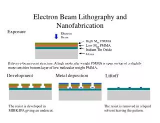
What is AIC? A process used to create polycrystalline silicon from amorphous silicon. This process consist of depositing a thin film of silicon and aluminum on a substrate and annealing the substrate between 150 to 400 degrees Celsius. 10 nm Al 200 nm Si Glass substrate
What is Annealing? • Annealing is a metallurgical heat treatment where in a material is altered, causing changes in the strength, hardness, and electrical properties of the material.
Why is AIC important? • It is an integral part of the process in the manufacturing of photovoltaic cells and Thin Film Transistors.
Mathematical Approximations of Surface Temperature E-beam Specific Heat Calculations Q= QAl + QSi Q= mAl CAl ΔT + mSiCSiΔT Q= (mAlCAl + mSiCsi)ΔT Q= (ρAlπr^2lAlCAl + ρSiπr^2lSiCSii)ΔT 10 nm Al ρAl = 2700 kg/m^3 ρSi = 2336 kg/m^3 lAl = 10 nm lSi = 200 nm CAl = 900 J/kg·k Csi = 703 J/kg·k r = to be determined by chart 200 nm Si
Methods and Materials Amorphous silicon Polysilicon E-beam
Results • We found that there was an affect from the electron beam on the surface of the substrate but that it was undetectable by XRD because of insufficient amount of polycrystalline silicon. After we switched to a substrate of smaller dimensions the change in the morphology of the surface was more defined. This amount was continuously of insufficient amount to be detected by XRD but there was a small amount of crystal growth detected by the TEM.
Acknowledgements • I would like to thank Dr.Hameed Naseem, Dr. Husam Abu-Safe, Mrs. Dorinne Bower, Mr. Ken Vickers, Mrs. Karla Clark and their associated programs along with the National Science foundation for the opportunity to do this summer research.