Download
1 / 42
540 likes | 1.04k Views
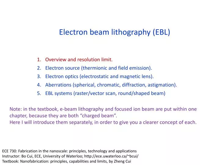
Electron beam lithography (EBL). Overview and resolution limit. Electron source (thermionic and field emission). Electron optics (electrostatic and magnetic lens). Aberrations (spherical, chromatic, diffraction, astigmation). EBL systems (raster/vector scan, round/shaped beam).

E N D
Electron beam lithography (EBL) Overview and resolution limit. Electron source (thermionic and field emission). Electron optics (electrostatic and magnetic lens). Aberrations (spherical, chromatic, diffraction, astigmation). EBL systems (raster/vector scan, round/shaped beam) Note: in the textbook, e-beam lithography and focused ion beam are put within one chapter, because they are both “charged beam”. Here I will introduce them separately, in order to give you a clearer concept of each. ECE 730: Fabrication in the nanoscale: principles, technology and applications Instructor: Bo Cui, ECE, University of Waterloo; http://ece.uwaterloo.ca/~bcui/ Textbook: Nanofabrication: principles, capabilities and limits, by Zheng Cui
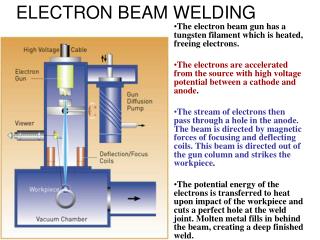
E-beam lithography (EBL) overview (direct writing with a focused e-beam) • Electron beam is focused to spot size <5nm using electron optics. • Very small wavelength: resolution less limited by diffraction. • Generate pattern by direct writing: ne need of mask or mold. • Sequential pixel-by-pixel writing: low throughput, unsuitable for mass production. For EBL at 30kV acceleration voltage =0.007nm For electron: (V is electron kinetic energy in eV) For light: For an electron with kinetic energy of 1eV, the associated DeBroglie wavelength is 1.23nm, about a thousand times smaller than a 1eV photon. (Note: electron rest mass energy is mc2=511keV, so relativity is unimportant for <50keV)
Exposure of resist • Typical energy for breaking a bond: 10eV • But typical energy of the e-beam: 10-100kV • (problems of aberration at low energy that leads to large beam spot size and low resolution, so use high energy for EBL) • Bond is broken by secondary (including Auger) electrons with low energy.
E-beam lithography facts • Developed in 1960s along with scanning electron microscope (SEM). • Breakthrough made in 1968 when a polymer called PMMA (poly methyl meth acrylate) was discovered to have high resolution. • Fast growth in 1990s when “nano” began to become “hot” and computer became more available for automatic lithography control. • Since around 2000, focused ion beam (FIB) patterning began to compete with EBL in some applications. • Today EBL is still the most popular nano-patterning techniques for academic research and prototyping.
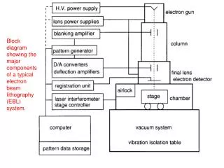
SEM/EBL system components • An electron gun or electron source that supplies the electrons. • An electron column that 'shapes' and focuses the electron beam. • A mechanical stage that positions the wafer under the electron beam. • (optional) A wafer handling system that automatically feeds wafers to the system and unloads them after processing. • A computer system that controls the equipment.
EBL systems: most research tools are based on SEM • E-beam writer • High energy column (100kV) • Dedicated electron optics • High reproducibility • Automatic and continuous (over few days) writing • High cost (>$5M) • Dedicated EBL system • Based on SEM system • With perfect integration • Interferometer stage • Focus correction (laser sample height control) • Cost $1-2M • SEM conversion • Conventional SEM (30kV) • Almost no SEM modification • Add beam blanker • Add hardware controller • Low cost: <$100K NPGS system Raith system Vistec system Beam blanker: is a DC bias (42V between two parallel plate electrodes) perpendicular to electron path, so that electrons are deflected away from the axis and thus “turned off”/blocked/blanked by the aperture below. The beam needs to be blanked so that it won’t expose the resist during its moving to next pattern location.
Electron beam lithography (EBL) Overview and resolution limit. Electron source (thermionic and field emission). Electron optics (electrostatic and magnetic lens). Aberrations (spherical, chromatic, diffraction, astigmation). EBL systems (raster/vector scan, round/shaped beam)
Electron guns/source Schematic structure of electron gun Electrons can be emitted from a filament (emitter or cathode) by gaining additional energy from heat or electric field. C: cathode for emitting electrons E: extraction electrode A1, A2: cathode lens electrode to focus the emitted electrons • Three types of electron guns: • Thermionic emission gun (W, LaB6, not-sharptip). • Field emission gun (cold, very sharp W tip, tunneling current). • Schottky gun (field assisted thermionic emission, sharp tip). • Whether it is field emission or not depends on the electric field near the tip apex, which determines whether tunneling is important or not. • Sharper tip leads to higher electric field near tip apex, so field emission (by tunneling) plays a major role, it is thus called field emission gun (FEG). • Even thermionic emission relies on the electric field from the extraction electrode, but here thermionic emission plays a major role.
Electron gun: thermionic emission (tungsten hairpin filaments) • The long time source of choice has been the W hairpin source • Working at high temperature, some electrons have thermal kinetic energy high enough to overcome the energy barrier (work function) • But kT still << work function 4eV). At 2000oC, • kT=1.3810-232273/1.610-19=0.20eV. • Escaped electron is then extracted by the electric field generated by the nearby electrode. • Current density Jcdepends on the temperature and cathode work function . • Cheap to make and use ($12.58 ea) and only a modest vacuum is required. Last tens of hours. Vacuum level W filament Work func-tion(eV) Thermionic electrons Schematic model of thermionic emission For a good introduction, go to: http://en.wikipedia.org/wiki/Thermionic_emission
Electron gun: thermionic emission (LaB6 tip) Richardson’s equation for emission current ( ) (Here work function is noted as EA, instead of ) Low work function, high melting point/T is good. LaB6 tip Besides W, single crystal LaB6 is another popular tip material for thermionic emission guns. About 5-10 more expensive than W, but last 5-10 longer and is brighter (higher beam current), but higher vacuum is required (since LaB6 is very reactive).
Field emission guns (FEGs) Field emitter tunneling Current density (Fowler-Nordheim equation ): J = A·F2·φ-1exp (-Bφ1.5/F) here A=1.510-6; B=4.5107; F>>108(V/m) • Field emission (i.e. tunneling) becomes dominant for electric field F>>108V/m. • Need very high vacuum to prevent arc-over at tip apex. • Strong nonlinear current-voltage characteristic. • Very short switching time (t<ns), since no need to heat up. • Small beam spot size, since field is high enough for tunneling only near tip apex.
Cold field emission guns (FEG) • Electrons “tunnel out” from a tungsten wire because of the high field (108V/cm) obtained by using a sharp tip (100nm) and a high voltage (3-4kV). • The emission current is temperature independent (pure tunneling current, operate at room temperature, so the name “cold”). • Needs ultra-high vacuum (UHV), but gives long life and high performance. Vacuum level Sharp tip, high electric field Work func-tion (eV) Field F (V/cm) Work function is lowered by , but this plays insignificant role for tunneling current.
Cold field emission gun (FEG) behavior • The tip must be very clean to perform properly as a field emitter. • Even at 10-6Torr, a monolayer of gas is deposited in just 1 sec. • So tip needs higher vacuum, 10-10Torr vacuum. • At this vacuum, the tip is usually covered with a mono- layer of gas in 5-10 minutes. • Cleaning is performed by “flashing” - heating the tip for a few seconds to desorbs gas. • The emission then stabilizes for a period of 2-5 hours. • On the stable region (hour 4 to hour 6), total noise + drift is a few percent over a few minutes, still not stable. (Right after flashing, current may drop 50% within a hour) • Flash is typically done automatically every morning, and SEM is good for 8-10 hours. • For e-beam lithography that need more stable current, good only during hour 4 to hour 8. • Because of the current instability, cold FEG is not good choice for e-beam lithography, though it is the best for SEM imaging applications. • Cold FEG is more expensive than Schottky emission guns, but last longer, up to 5 years.
Schottky emitters: field assisted thermionic source • Work function depends on temperature T and electric field F by: • Cathode behaves like a thermionic emitter with EA= 0-. Vacuum level ( ) Work func-tion (eV) For F=1108V/m, =0.38eV. Take T=1750K, then kT=0.15eV, current density is increased by: j/j0=e0.38/0.15=13. For F significantly higher than 1108V/m, the above equation is no longer valid since tunneling is becoming important. Field F (V/cm)
Schottky emitters: field assisted thermionic source • It is usually misleadingly called thermal or Schottky field emission guns. • But it is not a truly field emission gun, because the tip is blunt and if the heat is turned off there is no emission (tunneling) current. • A Schottky source is actually a field assisted (to lower ) thermionic source. Hitachi Schottky Emitter Tip (not sharp) • Schottky emitters can produce larger amounts of current compared to cold FEG systems, so more useful for e-beam lithography. • Because they are always on (hot, 1750K), organic contamination is not an issue (burned away immediately), hence they are very stable (few % per week change in current) • They eventually fail when the Zirconia reservoir is depleted, after 1-2 years. • Zirconia is used to further lower the (ZrO2has a low work function). <100> W crystal ZrO2 reservoir Polycrystalline W heating filament
Source size The cross-over is an effective real or virtual source for the downstream electron optical system. (real source) Cold field emission gun (cold FEG and Schottky) • The source size is the apparent width of the disc from which the electrons appear to come. • The tip physical size does NOT determine the source size. • Small is good for high resolution SEM, because less demagnification is needed to attain a given probe size. • But too small is not necessary, because anyway demagnification is needed to minimize effects of vibration and stray fields.
Source brightness • Brightness is defined as current per unit area per solid angle, with unit amp/cm2/steradian. • Brightness is the most useful measure of gun performance. • Brightness depends on energy, so one must compare different guns at the same beam energy (acceleration voltage). • High brightness is not the same as high current. • E.g. thermionic emission can have very high beam current, but low brightness (due to large d). Most current will then be blocked by a small aperture (to limit ) in order to have an acceptable small beam spot onto the specimen for high resolution imaging. e Measuring at the specimen
Relationship between probe current and probe diameter For typical EBL at 30kV, probe current is 20-1000pA. Cold field emission gives smallest beam spot size. However, for EBL the resolution is usually NOT limited by beam spot size (<10nm). It is more limited by lateral diffusion of secondary electrons and proximity effect due to backscattering. Very high current, but low brightness pA nA
Energy Spread • Electrons leave guns with an energy spread that depends on the cathode gun type. • Lens focus varies with energy (chromatic aberration, see later slides), so a high energy spread hurts high resolution images, as not all electrons are focused on the sample surface since they have different energy. • The energy spread of a W thermionic emitter is about 1.5-2.5eV. • For field emission and Schottky guns, the energy spread is about 0.3-0.7eV.
Comparison of electron emission sources Key parameters of electron sources: virtual source size, brightness, energy spread of emitted electron * (flashing) *Hitachi cold FEG SEM can go to 2nA.
Nano tips - atomic sized FEG Etched tungsten tip • Nano-tips are field emitters in which the size of the tip has shrunk to a single atom. • They can be made by processing normal tungsten field emission tips. • Or they are made from carbon nanotubes. • They can operate at energies as low as 50eV, and have a very small source size. • Field emission is significant at such a low voltage because the electric field is still high enough neat such a tiny tip apex. • The technique is not mature. Field ion image of a W nano-tip emitter
Regular and nano tips: comparison Copper alignment grid sample in S6000 CD-SEM Nano-tip Regular tip
Summary • The cold FEG offers high brightness, small size and low energy spread, but is least stable, generates limited current and must be flashed daily. • Schottky emitters are stable, reliable, with high resolution and beam current. So they are most popular for EBL. • Nano-tips may be the source of the future if they can be made reliably. • For imaging, W-hairpins or LaB6 guns (i.e. thermionic emission gun) are adequate for many applications not demanding highest resolution, or can operate at high acceleration voltage without sample damage/deformation (3nm imaging resolution at 30kV). • For e-beam lithography that always operates at relatively high voltage (typically 30kV for SEM conversion system), thermionic emission gun can be a reasonable inexpensive choice. • Cold field emission and Schottky gun SEM costs >2 that of thermionic gun SEM.
Electron beam lithography (EBL) Overview and resolution limit. Electron source (thermionic and field emission). Electron optics (electrostatic and magnetic lens). Aberrations (spherical, chromatic, diffraction, astigmation). EBL systems (raster/vector scan, round/shaped beam)
SEM/EBL electron optics Preparation of proper illuminating beam XY scanning Electron Optics Focusing objective Electron optics is not so obvious – not easy to predict electron trajectory, so one has to do numerical calculation.
Electrostatic lens Lens structure Electron trajectory Electric field Potential contour (100V) (0V) (0V) V3=0 V2 V1=0
Magnetic lens For rotationally symmetric magnetic field F=q v x B Uniform field Variable field • Magnetic lens good for focusing electrons, but not for ions with different charge/mass ratio. • Modern EBL uses only magnetic lens, since electrostatic lens using high field may lead to electrical breakdown at the gaps.
Electron beam lithography (EBL) Overview and resolution limit. Electron source (thermionic and field emission). Electron optics (electrostatic and magnetic lens). Aberrations (spherical, chromatic, diffraction, astigmation). EBL systems (raster/vector scan, round/shaped beam)
Aberrations • An ideal lens would produce a demagnified copy of the electron source at its focus. • The size of this spot could be made as small as desired. • But no real lens is ideal. • Aberration is defined as deviation from ideal case. • Geometric aberrations: spherical aberration, coma, field curvature, astigmatism and distortion. • Non-geometric aberrations: chromatic aberration, diffraction. • In light optics, the geometric aberration can be eliminated by changing arbitrarily the curvature of refractive surfaces. It may have hundreds of lens. • But in electron optics the electromagnetic field in space cannot be arbitrary changed. It has just a few lens.
Spherical aberrations • The focal length of near axis electrons is longer than that of off axis electrons. • All lenses have spherical aberration, with minimum spot size • ds = 0.5Cs3 • Cs is a lens constant related to the working distance of the lens. (minimizing working distance minimizes spherical aberration). • Spherical aberration makes the probe larger and degrades the beam profile. • To reduce it, one needs to limit the numerical aperture () of the probe lens; but this also reduces the current IB that varies as 2. DOLC Gaussian focus plane DOLC: disk of least confusion
Chromatic aberrations • The focal length of higher energy electrons is longer than that for lower energy electrons. • The minimum spot size at DOLC is • dc= CcE/E0 (or V/V) • which is high at low energies E0, or when using thermionic emitters with high energy spread E. DOLC DOLC: disk of least confusion
Diffraction • Electrons are waves so at focus they form a diffraction limited crossover. • The minimum diameter dd=0.61/NA=0.61/sin0.61/ • (Rayleigh criteria, same as optical lens). • At low energies the wavelength becomes large (0.04 nm at 1keV) so diffraction is a significant factor because is typically only 10 milli-radians or less in order to control spherical and chromatic aberrations
Astigmation Minimum spot size da=Ca Astigmation: focal points for x- and y-directions are different Beam shape at different planes • Every time one switch on or adjust an electron lens (magnetic, not electrostatic lens), the magnetization of the metal in the lens changes. • Because of hysteresis, the lens never quite goes back to where it was. • The lens will then have non-round features due to different magnetization around the pole-piece, which is the focusing part of the electron lens. • Apertures tend to charge up if they have dirt on them, leading to another source of asymmetry. • Stigmators eliminate/compensate astigmation by adding a small quadrupole distortion to the lens. • When beam is well optimized, astigmation causes negligible beam spot broadening.
Overall beam spot diameter (assume no astigmation) dv: virtual source diameter M (>1): demagnefication Spherical aberration Chromatic aberration Diffraction • Beam spot size depends on acceleration voltage, because higher voltage/energy leads to: smaller chromatic aberration, and shorter thus smaller diffraction. • This is particularly true for thermionic emission guns, where high resolution (<5nm) can only be achieved at near 30kV. • Such resolution can be achieved at <5kV for cold field emission and Schottky guns.
Beam spot diameter: a real example total beam diameter spherical source size limit diffraction chromatic • is determined by aperture size (10-100m), which should be selected wisely. • Typically beam diameter is NOT the limiting factor for high resolution, then large is good for high beam current and thus fast writing. • But large also reduces depth of focus (1/2), leading to large beam spot size (low resolution) if beam is not well focused due to wafer non-flatness or tilt.
Electron beam lithography (EBL) Overview and resolution limit. Electron source (thermionic and field emission). Electron optics (electrostatic and magnetic lens). Aberrations (spherical, chromatic, diffraction, astigmation). EBL systems (raster/vector scan, round/shaped beam)
Raster scan vs. vector scan Raster scan: The e-beam is scanned in only one direction with beam blanking, and the stage ismechanically translated in the perpendicular direction. Vector scan: The e-beam is scanned in both x- and y-directions with beam blanking, writing the pattern pixel-by-pixel. No stage movement within each writing field. After each writing field, the substrate/stage moves to the next location.
Raster scan versus vector scan Raster scan • Raster scan: • Very simple and fast. • Very repeatable • But sparse patterns take as long as dense patterns. • Difficult to adjust dose during writing. • For photo-mask making. Beam blanked here Vector scan • Vector scan: • Fast writing of sparse patterns (unwritten areas skipped). • Easy dose variation from shape to shape. • For nanolithography and R&D. Beam never pass here
Round (Gaussian beam) vs. shaped beam • Beam is shaped to a rectangular shape for fast writing. • Fast since each “pixel” is large. • Mainly used for photo-mask making, with each square pixel size order 100nm. • Beam is focused to a round spot with size as small as possible for high resolution. • Slow since each pixel is small (order 10nm). • Used for R&D. Gaussian beam shaped beam
Laser interferometer stage • For conventional SEM, stage accuracy is about 5μm, so good alignment is not possible. • Precise alignment of different layers requires local alignment marks (like photolithography). • For advanced EBL system, use interferometry to precisely position the stage. • Better than 5nm positioning accuracy, thus different writing fields are nearly perfectly aligned (“stitched”). • Interferometry stage cost $0.5-1M, as expensive as a SEM. • Using laser beam, sample height can also be monitored to maintain focusing/constant sample height.