Download
1 / 30
300 likes | 475 Views
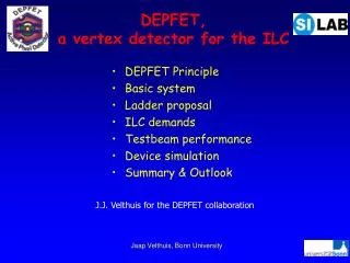
DEPFET Status. DEPFET Principle Readout modes Projects: XEUS WIMS ILC ILC Testbeam results Summary & Outlook. Univ. of Bonn: M.Karagounis, R.Kohrs, H.Krüger, M. Mathes, L.Reuen, C.Sandow, E.von Törne, M.Trimpl, J.Velthuis, N.Wermes Univ. of Mannheim: P.Fischer, F.Giesen, I.Peric

E N D
DEPFET Status • DEPFET Principle • Readout modes • Projects: • XEUS • WIMS • ILC • ILC Testbeam results • Summary & Outlook Univ. of Bonn: M.Karagounis, R.Kohrs, H.Krüger, M. Mathes, L.Reuen, C.Sandow, E.von Törne, M.Trimpl, J.Velthuis, N.Wermes Univ. of Mannheim: P.Fischer, F.Giesen, I.Peric Politecnico di Milano: M. Porro MPI Halbleiterlabor Munich: O Hälker, S. Herrmann,L.Andricek, G.Lutz, H.G. Moser, R.H.Richter, M.Schnecke, L.Strüder, J.Treis, P.Lechner, S. Wölfel THCA of Tsinghua Univ.: C. Zhang, S.N. Zhang Vertex05, 8/11/05 Jaap Velthuis, Bonn University
A p-FET transistor is integrated in every pixel. By sidewards depletion potential minimum created below internal gate. Electrons, collected at internal gate, modulate transistor current MIP source top gate drain clear bulk n+ p+ p+ n+ n+ ~1µm p s n i x internal gate a y r t 50 µm e + - - m - - - m - - y + s - - n + + - p+ rear contact DEPFET Principle Vertex05, 8/11/05 Jaap Velthuis, Bonn University
DEPFET Principle • Advantages: • Fast signal collection due to fully depleted bulk • Low noise due to small capacitance and amplification in pixel • Transistor can be switched off by external gate – charge collection is then still active ! • Non-destructive readout • Disadvantages: • Need to clear internal gate. This still requires high voltages. • 2 readout modes: • Source follower mode readout. Signal is voltage (XEUS) • Drain readout. Signal is current (WIMS&ILC) required Vertex05, 8/11/05 Jaap Velthuis, Bonn University
Gate DEPMOS device Drain Source Buffer / amplifier Clear- gate Ibias Clear Ibias SOURCE FOLLOWER • Constant bias current IBias provided • Charge at internal gate translates into source voltage node change • Speed depends on overall load capacitance • Slow (t≈CL/gm≈3µs), but excellent noise Vertex05, 8/11/05 Jaap Velthuis, Bonn University
CURO: current amplifier DEPMOS device Gate Source Drain Vout transimpedence amplifier Clear- gate Clear DRAIN readout • Measure Idrain directly • Fast response: limited by RC time of input resistance CURO and Cload (~ns) Vertex05, 8/11/05 Jaap Velthuis, Bonn University
DEPFET Applications • DEPFET under study for: • XEUS • Exploring the early universe by imaging spectroscopy in the X-ray band • Need noise < 4e- • Source follower mode • WIMS • Wide-band Imaging and Multi-band Spectrometer, part of China’s spacelab mission • Drain readout • ILC • Need row rates of 20MHz • Drain readout Vertex05, 8/11/05 Jaap Velthuis, Bonn University
XEUS • Exploring the early universe by imaging spectroscopy in the X-ray band • Detector: • Device active area 7.68 x 7.68 cm2 • Monolithic sensor integrated onto a single 6“ wafer • Device thickness 450 µm • Pixel size 75 x 75 µm2 • Position resolution ca. 30 µm • Total 1024 x 1024 pixel cells • Total readout time / frame 1.25 ms • Processing time per detector row 2.5 µs Vertex05, 8/11/05 Jaap Velthuis, Bonn University
Excellent noise • Single pixel device • 10 µs shaping • Room temperature (22° C) Vertex05, 8/11/05 Jaap Velthuis, Bonn University
Noise dependence • Pixel readout noise: 63 – 14eV (17 – 3.6 e- ENC) Energy resolution: 126 eV FWHM @ Mn-Ka Line corresponding to 4.9 e- ENC Excellent noise • Large structure (64x64): • 75 x 75 µm2 pixel size • 45 µm gate circumference / 5 µm gate length • Drain in center of pixel • Cut gate geometry • Curved edge • Double metal • Operated at: • Pixel current 30 µA • Line processing time 25 µs Vertex05, 8/11/05 Jaap Velthuis, Bonn University
Room temperature Back side illuminates, fast drain readout Shaping time: 3μs Clear pulse period 1 ms with width 3 μs WIMS • Wide-band Imaging and Multi-band Spectrometer (WIMS) is part of China’s spacelab mission . • Observe high-energy bursts, transients and fast-varying sources over a broad spectral range simultaneously • Using Macro pixels • Pixel size 0.5x0.5 mm2 • “Si-drift chamber readout using DEPFET” Vertex05, 8/11/05 Jaap Velthuis, Bonn University
DEPFET for ILC • Basic system • Clearing • ILC requirements • Ladder proposal • Power consumption • Thinning • Radiation hardness • Testbeam results Vertex05, 8/11/05 Jaap Velthuis, Bonn University
Gate Switcher DEPFET Matrix 64x128 pixels, 36 x 28.5µm2 Clear Switcher Current Readout CUROII Basic system • Select and Clear signals provided by SWITCHER • 64 x 2 outputs • Max ΔV = 25V • Read out row-wise: CURO • current based read out • 128 channels • CDS • real time hit finding & zero-suppression • row rate up to 24 MHz Vertex05, 8/11/05 Jaap Velthuis, Bonn University
HighE vs non-HighE • HighE extra n-type implant • Moves internal gate deeper into bulk • Clearing takes places deeper in the bulk • Lower signals, but easier clearing clear channel Internal gate Optional HighE implant Vertex05, 8/11/05 Jaap Velthuis, Bonn University
Clearing HighE • CURO measures: Isig,i+Iped,i & Iped,i+1 • Need to remove all charge such that Iped,i+1=Iped,i • COMPLETE CLEAR possible for HighE with low voltages (~7V)⇒ possible to make radhard SWITCHER in standard CMOS Vertex05, 8/11/05 Jaap Velthuis, Bonn University
ILC requirements • Time structure: 1 train of 2820 crossings in ~1 ms every ~200ms • Hit density: for r = 15 mm: ~ 100 tracks / mm2 / train • Row readout rate: > 20 MHz • Occupany < 0.5 % • Radiation length: ~0.1% X0 per layer • thinned sensors (50 μm) • low power consumption • Radiation tolerance: 200 krad (for 5 years operation) • Resolution: few µm ( pixel size ≤ 25 x 25 µm2) Vertex05, 8/11/05 Jaap Velthuis, Bonn University
Ladder proposal • Modules have active area ~13 x 100 mm2 • Read out on both sides. • Detectors 50µm thick, with 300µm thick frame yields 0.11% X0 • SWITCHER & CURO chips connected by bump bonding CURO SWITCHER Vertex05, 8/11/05 Jaap Velthuis, Bonn University
ILC Power • Measured Power Dissipation: • Switcher: 6.3 mW per active channel at 50MHz • CURO: 2.8 mW / channel • Assumed Power Dissipation of DEPFET Sensor: • 0.5 mW per active pixel • duty cycle: 1/200 • Only active pixel dissipate power • 1024 active pixels per module • 8 modules in Layer 1 => 8192 active pixels • Expected Power Dissipation in Layer 1 • Sensor: 8192 x 0.5 mW / 200 = 20 mW • Switcher: 16 x 6.3 mW / 200 = 0.5 mW • Curo: 8192 x 2.8 mW / 200 = 114 mW • For Layer 1 Sum: 135 mW For 5 Layer DEPFET Vertex Detector:Total ~ 3.6 W no active cooling Vertex05, 8/11/05 Jaap Velthuis, Bonn University
sensor wafer handle wafer 2. bond wafers with SiO2 in between 3. thin sensor side to desired thick. 4. process DEPFETs on top side 5. etch backside up to oxide/implant 1. implant backside on sensor wafer first ‘dummy’ samples: 50µm silicon with 350µm frame thinned diode structures: leakage current: <1nA /cm2 Thinning Thinning technology for active area established Vertex05, 8/11/05 Jaap Velthuis, Bonn University
60Co Radiation hardness • Irradiations with 60Co and X-rays (~17keV) up to ~1Mrad (SiO2) • Threshold shift of the MOSFET (~4V) can be compensated by bias voltage shift Vertex05, 8/11/05 Jaap Velthuis, Bonn University
1 2 3 4 Scintillator DEPFET Scintillator 3 x 3 mm² beam Testbeam • DESY test beam with 6 GeV e- • Bonn ATLAS telescope system: • double sided strip detectors • pitch 50 µm (no intermediate strips) • readout rate 4.5 kHz (telescope only) • DEPFET: • 128x64 (28.5x36 µm2) • 450 µm thick • Frame time 1.8 ms Vertex05, 8/11/05 Jaap Velthuis, Bonn University
Pedestal & Noise • Pedestal: average signal after hit removal • Noise: standard deviation after pedestal, common mode and hit removal Vertex05, 8/11/05 Jaap Velthuis, Bonn University
Clustering • Look for clusters: • Seed • pixel largest signal • seed cut >5σ • Neighbours • Neighbour cut >2σ • Combine signals seed & neighbors • S/N3x3=125.9±0.2 • Noise higher than expected • Next generation expect to reduce noise by factor 2 Vertex05, 8/11/05 Jaap Velthuis, Bonn University
Position resolution • Hit positions reconstructed using the CoG algorithm • Note: pixelsize X=36µm Y=28.5µm • Terrible, but … due to multiple scattering Vertex05, 8/11/05 Jaap Velthuis, Bonn University
Multiple scattering • Eelectron only 6GeV • Telescope planes 10cm apart • Minimize effect scattering by selecting hard tracks using 2 cut • Price: lose statistics Vertex05, 8/11/05 Jaap Velthuis, Bonn University
Multiple scattering (II) • Performed simulation. • Using Fraction remaining tracks, telescope uncertainty can be estimated. • From CERN testbeam know that σintrinsic~5-6µm, but not compared S/Ntel • σX=9.71±0.02µm, σY=9.31±0.02µm Vertex05, 8/11/05 Jaap Velthuis, Bonn University
Poor stats & fit HighE matrix • HighE implant moves internal gate into bulk • Lower signal • Easier clearing • Results: • S/N3x3=99.5±0.1 • σX=9.11±0.03µm, σY=8.80±0.03µm • Somewhat larger clusters yield better position resolution Vertex05, 8/11/05 Jaap Velthuis, Bonn University
Summary • DEPFET integrates MOSFET in fully depleted bulk. Developed towards: • XEUS mission: • Slow readout (source follower mode) • Excellent noise (~2.2e-) • WIMS mission • Very large pixels (0.5x0.5mm2) • Si-drift chamber readout by DEPFET • Fast(er) readout (noise=19e-) Vertex05, 8/11/05 Jaap Velthuis, Bonn University
Summary (II) • Developed towards ILC. Meets already demands on • Radiation length (0.11 X0) • Radiation hardness (ΔVth shift~4V@1Mrad) • Power consumption (<5W full detector) • Position resolution (≲5µm) • Excellent S/N: • S/N=126 without HighE • S/N=100 with HighE • ⇒can thin detector to 50µm with still good S/N Vertex05, 8/11/05 Jaap Velthuis, Bonn University
Outlook • Improving the system to increase readout speed. • Individual parts already function well at ILC speed • Testbeam at DESY (6GeV electrons) with better mechanics and at CERN. Goals: • Improve S/N • Test zero suppression • Build 512x512 matrix Vertex05, 8/11/05 Jaap Velthuis, Bonn University
Author list Univ. of Bonn: M.Karagounis, R.Kohrs, H.Krüger, M. Mathes, L.Reuen, C.Sandow, E.von Törne, M.Trimpl, J.Velthuis, N.Wermes Univ. of Mannheim: P.Fischer, F.Giesen, I.Peric Politecnico di Milano: M. Porro MPI Halbleiterlabor Munich: O Hälker, S. Herrmann,L.Andricek, G.Lutz, H.G. Moser, R.H.Richter, M.Schnecke, L.Strüder, J.Treis, P.Lechner, S. Wölfel THCA of Tsinghua Univ.: C. Zhang, S.N. Zhang Vertex05, 8/11/05 Jaap Velthuis, Bonn University