Download
1 / 77
770 likes | 783 Views
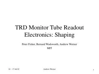
DEPFET Readout Electronics. Ivan Peric, Jochen Kinzel, Christian Kreidl, Peter Fischer University of Heidelberg. Introduction. Switcher. DCD. DHP. DHP. DEPFET readout and control-ASICS. Switcher – row control chip with high voltage line drivers 0.35 μ m technology

E N D
DEPFET Readout Electronics Ivan Peric, Jochen Kinzel, Christian Kreidl, Peter Fischer University of Heidelberg
Switcher DCD DHP DHP DEPFET readout and control-ASICS Switcher – row control chip with high voltage line drivers 0.35 μm technology DCD – DEPFET current receiver and digitizer chip 0.18 μm technology DHP – Digital data handling and readout control chip 0.09 μm technology ACTIVE AREA (32 channels each) Chip 960X512 Bump bonding Switcher#4 Sensor – active area Sensor balcony Switcher#0 DCD#0 – DCD#5 (160 channels each) Fan-out
interdigitated AC coupling caps 80µm opening Ivan Peric, Mannheim HV channel with 3+3 Switch transistors and 4 AC coupling stages (180x180µm, M4 not shown) Switcher with LV transistors – Switcher 3 Switcher 3 Radiation tolerant layout in 0.35 μm technology 128 channels + Very fast - Operation up to 11.5 V Novel design: Uses stacked LV transistors, HV twin-wells and capacitors as level-shifters + No DC power consumption - SEU causes shorts
Switcher 3 – output driver • Use an SRAM cell flipped by a transient voltage • No dc power consumption! 9V ‘SRAM’ 6V ‘SRAM’ 3V out 6V ~200 fF ‘SRAM’ Reset 3V ‘SRAM’ 0V
Switcher 4 Switcher 3 Uses radiation tolerant high voltage transistors in HV 0.35 μm technology 64 channels - Not as fast + Possible operation up to 50 V (30V tested) - moderate DC power consumption (32 X 30uA X 12V = 11.52mW) Enclosed design of NMOS HV transistors
Switcher 4 chip – high voltage transistors Thick oxide 17-20V Thin oxide 0-3V 0-20V 20V 0V p- n- Hi voltage Hi voltage Hi voltage n- Hi voltage p- PMOS Vertical NMOS
G Difefrent types of radiation-soft and -hard NMOS transistors Thick oxid Leakage current G D G D B S S S Standard NMOS Annular gate NMOS D Annular gate vertical NMOS
Switcher 4 chip output driver 20V 17V logic out in 3V 0V
DCD3 chip • - Technology 0.18 μm • - 72 Channels • - 2 ADCs and regulated cascode/channel • - 6 channels multiplexed to one digital LVDS output • - ADC sampling period 160 ns (8 bits) • - Channel sampling period 80 ns • - LVDS output: 600 M bits/s • - Chip: 7.2 G bits/s (12 outputs) • - Radiation tolerant design • - ~ 1mW/ADC (optimal powering) • - ~ 1mW/Cascode
DCD 3 measurements ADC characteristic Noise
Gate On DCD3 ADC 1 1 2 2 DEPFET 3 3 4 4 5 5 6 6 7 7 7 7 W R NC R R L Reg. cascode 7 R L 5 5 6 6 7 7 7 7 6 6 5 5 4 4 W 3 3 W R R NC R Double sampling R L 3 R L
DCD conversion principle A1 A2 S O B1 B2 S S S 2S-R S 2S-R S S S 2S-R
DCD conversion principle sample state 1 sample state 2 state3 state4 memory cell S S h0 l0 comparator nc c c wr rd lt lt rd rd lt lt rd wr r r nc States: 1. 2. 1. 2. rd – read wr – write nc – not connected r – reset c – compare lt - latched nc lt lt nc wr r r nc nc c c wr nc lt lt nc 3. 4. 3. 4. 2(S-h0R+l0R) 2(S-h0R+l0R) ck1 ck2 ck3 ck4 state1 state2 state3 state4 sample state 1 S‘ 2(2(S-h0R+l0R)-h1R+l1R) h2 l2 nc c c wr rd lt lt rd rd lt lt rd wr r r nc wr r r nc rd lt lt rd wr r r nc nc c c wr rd lt lt rd nc lt lt nc h3 l3 h1 l1 2(2(2(S-h0R+l0R)-h1R+l1R)–h2R+l2R) ck5 ck6 ck7 ck8 ck9 2(2(2(2(S - h0R + l0R) - h1R + l1R) – h2R + l2R) – h3R + l3R) = Res Res
Timing 80ns Gate Current 25ns 25ns Clear S Wr S B1 B2 S A1 A2 Wr O
Channel geometry Power line Data compression Current receiver Logic 1000uA Pad 110um 180um
Improvements • Dynamic range (radiation damage) • Speed (background) • Pickup noise immunity (environmental noise) • Noise (presently 100e) • Geometry (compatibility with solder bump technologies) • Power (cooling, voltage drops) • Dynamic Range: DKS with large input cell, modified ADC algorithm, scaled pipeline ADC • Sample speed: Single sampling, clear without return to baseline • ADC speed: pipeline ADC • Noise: DKS with single sampling cell, single sampling • Pickup noise immunity: DKS, differential readout • Power: Simplified comparator, resistance instead SF
Improvements – large Input cell/modified algorithm A1 A2 S O S B1 S B2 ADC with large input cell S S S S 2S-R S 2S-R S S S 2S-R Original algorithm S/2 S/2 S/2 S-R S/2 S-R S/2 S/2 S/2 S/2 S-R Modified algorithm
Original algorithm sample state 1 sample state 2 state3 state4 memory cell S S h0 l0 comparator nc c c wr rd lt lt rd rd lt lt rd wr r r nc States: 1. 2. 1. 2. rd – read wr – write nc – not connected r – reset c – compare lt - latched nc lt lt nc wr r r nc nc c c wr nc lt lt nc 3. 4. 3. 4. 2(S-h0R+l0R) 2(S-h0R+l0R) ck1 ck2 ck3 ck4 state1 state2 state3 state4 sample state 1 S‘ 2(2(S-h0R+l0R)-h1R+l1R) h2 l2 nc c c wr rd lt lt rd rd lt lt rd wr r r nc wr r r nc rd lt lt rd wr r r nc nc c c wr rd lt lt rd nc lt lt nc h3 l3 h1 l1 2(2(2(S-h0R+l0R)-h1R+l1R)–h2R+l2R) ck5 ck6 ck7 ck8 ck9 2(2(2(2(S - h0R + l0R) - h1R + l1R) – h2R + l2R) – h3R + l3R) = Res Res
Modified algorithm sample state 1 sample state 2 state3 state4 memory cell S h0 l0 comparator nc c c nc rd lt lt rd rd lt lt rd wr r r wr States: 1. 2. 1. 2. rd – read wr – write nc – not connected r – reset c – compare lt - latched nc lt lt nc wr r r nc nc c c wr nc lt lt nc 3. 4. 3. 4. 2(S/2-h0R+l0R) 2(S/2-h0R+l0R) ck1 ck2 ck3 ck4 state1 state2 state3 state4 sample state 1 S‘ 2(2(S/2-h0R+l0R)-h1R+l1R) h2 l2 nc c c wr rd lt lt rd rd lt lt rd wr r r nc wr r r nc rd lt lt rd wr r r nc nc c c wr rd lt lt rd nc lt lt nc h3 l3 h1 l1 2(2(2(S/2-h0R+l0R)-h1R+l1R)–h2R+l2R) ck5 ck6 ck7 ck8 ck9 2(2(2(2(S/2 - h0R + l0R) - h1R + l1R) – h2R + l2R) – h3R + l3R) = Res Res
DKS vs. single sampling DKS Gate Current after cascode 25ns Clear so s Sample 80ns Single sampling s s 55ns
Fast clear DKS Gate Current after cascode 25ns Clear so s s Sample 75ns Single sampling s s 50ns
Fast clear – switcher modification AND D ld Reset
Double-cell DKS S O Noise ~ 100e B1 A1 LSB ~ 160e B2 A2 80ns Gate Current 25ns 25ns Clear Wr S B1 B2 A1 A2 Wr O
Single-cell DKS Noise ~ 100e/1.41 S B1 A1 LSB ~ 160e B2 A2 80ns Gate Current 25ns 25ns Clear Wr S B1 B2 A1 A2
Single-cell DKS Noise ~ 100e/1.41 S B1 A1 LSB ~ 320e B2 A2 80ns Gate Current 25ns 25ns Clear Wr S B12 A12
Single-cell DKS Noise ~ 100eX1.41 S S B1 A1 LSB ~ 320e S S B2 A2 80ns Gate Current 25ns 25ns Clear Wr S B12 A12
ADC Cell Lo Hi C1 C2 Rd Logic AmpLow WrB* R Add Sub AmpLow RdB WrB 24 μA 6X2 μA Rd 12 μA Wr Vbias RefIn 24 μA To Comp In? Or use Th instead Gate
ADC Cell – low-power scheme Lo Hi C1 C2 Rd Logic AmpLow WrB* R Add Sub AmpLow RdB WrB 24 μA 6X2 μA Rd 12 μA Wr Vbias RefIn 24 μA To Comp In? Or use Th instead Gate
Comparator ResB LB Or th ResB RefIn L Th Comp In AmpLow 24 μA 6X2 μA 12 μA Vbias 24 μA Gate
Comparator – low-power scheme ResB LB Or th ResB RefIn L Th Comp In AmpLow 24 μA 6X2 μA 12 μA Vbias 24 μA Gate
Cascode 40 μA 1.8 V 1 mA Vbias 1 V 0.3 mA
Pixel difference readout a b c d a b c d a b - - 4pixels/80ns 4pixels/40ns a > th ? (a - hit : a - not hit) a-b > 0 ? (a - hit : b - hit)
Pixel difference readout vs standard readout • + Differential readout – immune against pickup – operation without DKS possible, no need for common mode correction • + 2X less ADC channel needed • + doubled conversion speed by the same number of ADC cores • + if used without DKS sampling speed can be doubled • + compatible with standard readout • - lost hits when both coupled pixels generate the same signal • - by one reduced number of bits (7 vs 8 bits) • - in the case of used DKS, larger noise by 1.41
Connection scheme 16-19 0 4 16 20 24 1 5 17 21 2 6 18 22 3 7 19 23 27 4-7 24-27 0-3 20-23
Lost hits Not detected Detected 0 4 16 20 24 0 4 16 20 24 1 5 17 21 1 5 17 21 2 6 18 22 2 6 18 22 3 7 19 23 27 3 7 19 23 27 Detected Detected 0 4 16 20 24 0 4 16 20 24 1 5 17 21 1 5 17 21 2 6 18 22 2 6 18 22 3 7 19 23 27 3 7 19 23 27
Scheme with error correction a+b-(c+d)? a b c d <0 >0 =0 a or b c or d ac, ad, bc, bd or none + - c-d? a-b? + d c b a - - cd ab c-d? ad, bd ac, bc 4pixels/40ns a-b? a-b? none bd ad bc ac
Channel geometry Power line Data compression Current receiver Logic Pad 110um 180um
Channel geometry 110um 185um
Channel geometry 110um 160um
1:1 1:1.5 150 um 10X16 150 um 150 um 8X20 190 um
10X16 geometry Digital Part