Download
1 / 17
170 likes | 294 Views
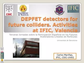
DEPFET Technology for future colliders. Carlos Mariñas IFIC-Valencia (Spain). 1. DEPFET ( DEpleted P- channel Field Effect Transistor): Technology invented by J. Kemmer & G. Lutz , 1987

E N D
DEPFET Technology for future colliders Carlos Mariñas IFIC-Valencia (Spain) 1 Carlos Mariñas, IFIC, CSIC-UVEG
DEPFET (DEpleted P-channelFieldEffect Transistor): Technologyinventedby J. Kemmer & G. Lutz, 1987 • J. Kemmer and G. Lutz: ''New semiconductor detector concepts'', Nucl. Instr. & Meth. A 253 (1987) 365-377 • SeveraldifferentapplicationsforAstrophysics and ParticlePhysics: • XEUS: Futureeuropean X-rayobservatorytoinvestigate the Early Evolution Stages of the Universe (early black holes, evolution of galaxies…) • BepiColombo: ESA projectto Mercury toinvestigatetheorigin and evolution of theplanet • X-FEL • ILC • BELLE-II → Technologychosenforthe new Vertex Detector 2 Carlos Mariñas, IFIC, CSIC-UVEG
Why this technology? • Vertexing in futurecollidersrequiresexcellentvertexreconstruction and efficient heavy quark flavourtagging • See Prof. Ch.Damerell’stalk • Thisrequirementsimposeunprecedentedconstraintsonthe detector: • Highgranularityto cope withthehighdensity of tracks in the jets and thebackground • Highspatialresolution per layer <4mm (pixel size of 25x25mm2) • Fastread-out • Low material budget: <0.1%X0/layer (~100mm of Si) • Lowpowerconsumption • DEPFET • Measurementsmadeonrealistic DEPFET prototypeshavedemonstratedthatthe concept isone of the principal candidatestomeetthesechallengingrequirements 3 Carlos Mariñas, IFIC, CSIC-UVEG
The DEPFET principle • Each pixel is a p-channel FET on a completelydepletedbulk (sidewarddepletion). Chargeiscollectedbydrift • A deep n-implantcreates a potentialminimumforelectronsunderthegate (internalgate) • Signalelectronsaccumulate in theinternalgate and modulatethe transistor current (gq≈500pA/e-) • Accumulatedcharge can be removed by a clearcontact • Small pixel size~25μm • r/o per row ~50ns (20MHz) (drain)Fullydepletedbulk • Noise≈100e-Small capacitance and first in-pixel amplification • Thin Detectors≈50μm • Internalamplification • Low power consumption: Readout on demand (Sensitive all the time, even in OFF state) GOAL 4 Carlos Mariñas, IFIC, CSIC-UVEG
MIP source top gate drain clear bulk n+ p+ p+ n+ n+ p n s i internal gate x a + - - y - - - r t - - e + m - m y s + - n + - p+ rear contact DEPFET-Principle of Operation Potential distribution: internal Gate ~1µm Backcontact Drain 50 µm Source [TeSCA-Simulation] FET-Transistor integrated in every pixel (first amplification) Electrons are collected in „internal gate“ and modulate the transistor-current Signal charge removed via clear contact 5 Carlos Mariñas, IFIC, CSIC-UVEG
source top gate drain clear bulk +20V n+ p+ p+ n+ n+ 0V 0V p n s i internal gate x a - - y - - - r t - e m m y s - n p+ rear contact DEPFET-Principle of Operation Potential distribution: internal Gate ~1µm Backcontact Drain 50 µm Source [TeSCA-Simulation] FET-Transistor integrated in every pixel (first amplification) Electrons are collected in „internal gate“ and modulate the transistor-current Signal charge removed via clear contact Carlos Mariñas, IFIC, CSIC-UVEG
ILC prototype system • HybridBoard • DEPFET 64x256 matrix • Readout chip (CURO) • Steering chips (Switchers) • ProtectionBoard • Regulators • ReadoutBoard • 16 bit ADCsDigitization • XILINX FPGAChipconfig. and synchronizationduring DAQ • 128 kBRAMDatastorage • USB 2.0 boardPCcomm. 6 Carlos Mariñas, IFIC, CSIC-UVEG
Hybrid board Clear sw gaTEsw DEPFET Curo • DEPFET Matrix • 64x128 pixels • Several pixel sizes, implants, geometries • CURO: • 128 channels • CUrrentReadOut • Subtraction of IpedfromIped+Isig • Switchers: • Steering chips • Gate: Selectrow • Clear: Clear signal 7 Carlos Mariñas, IFIC, CSIC-UVEG
Operation mode: Row wise readout Clear SW DEPFET-matrix Gate SW Row wise r/o (Rolling Shutter) • Select row with external gate, read current, clear DEPFET, read current again The difference is the signal • Low power consumption: Only one row active at a time; Readout on demand (Sensitive all the time, even in OFF state) • Two different auxiliary chips needed (Switchers) • Limited frame rate Drain Enable row – Read current (Isig + Iped) – Clear – Read current (Iped), Subtract – Move to next row 8 Carlos Mariñas, IFIC, CSIC-UVEG
DEPFET Concept for a half ILC module • 10 and 25 cm long ladders read out at the ends • 24 micron pixel • design goal 0.1% X0 per layer in the sensitive region 9 Carlos Mariñas, IFIC, CSIC-UVEG
Thinning : mechanical samples 6” wafer with diodes and large mechanical samples Thinned area: 10cm x 1.2 cm (ILC vertex detector dummy) Possibility to structure handling frame (reduce material, keep stiffness) 10 Carlos Mariñas, IFIC, CSIC-UVEG
DEPFET achievements: Test Beam Setup x z y • Telescope: • 5 DEPFET planes • 32x24μm2 • CCG • 450 μm thick BEAM • DUT: • 1 DEPFET modules • Various pixel sizes • 450 μm thick 120 GeV ∏ • Scintillators: • 1 Big “Beamfinder” • 1 Finger “Beamallignment” • Triggering Trigger Synchronization via TLU(Trigger Logic Unit) 11 Carlos Mariñas, IFIC, CSIC-UVEG
Test Beam Setup • General view • 6 Modules at once • 1 rotating module 12 Carlos Mariñas, IFIC, CSIC-UVEG
My work • Calibration/optimization of differentgenerations of matrices: • PXD4-Clocked Cleargate. 128x64 pixels • PXD5-Common Cleargate. 128x64 pixels • PXD5-Capacitative CoupledCleargate. 256x64 pixels 13 Carlos Mariñas, IFIC, CSIC-UVEG
3x3 clustersignal • Test Beam • Data analysis (SNR, Residuals, Chargecollectionuniformity) σ≈4% ResY=1.34μm Preliminary 14 Carlos Mariñas, IFIC, CSIC-UVEG
Mechanical/Thermalmeasurements and simulation (FiniteElementAn.) • Natural frequencies, selfweigthbowing, deformations • Conduction, convection, thermalstress • Powercycling • Thermalcharacterization of differentmaterialsforcooling (Al, Cu, TPG) Natural convection 15 Carlos Mariñas, IFIC, CSIC-UVEG
Belle-II, SuperB, ILC, CLIC… Thank you very much! • The LHC is not the end… but just the beginning! 16 Carlos Mariñas, IFIC, CSIC-UVEG