Download
1 / 59
590 likes | 726 Views
DEPFET Readout and Control Electronics. Ivan Peric, Peter Fischer, Christian Kreidl Heidelberg University. Outline. Module Electronics - Introduction Principle of DEPFET readout Switcher with LV transistors (Switcher 3) Switcher with HV transistors DCD Chip Bumping technologies.

E N D
DEPFET Readout and Control Electronics Ivan Peric, Peter Fischer, Christian Kreidl Heidelberg University DEPFET Electronics
Outline • Module Electronics - Introduction • Principle of DEPFET readout • Switcher with LV transistors (Switcher 3) • Switcher with HV transistors • DCD Chip • Bumping technologies DEPFET Electronics
DEPFET readout and control-ASICS DEPFET Electronics
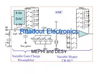
Switcher DCD DHP DHP DEPFET readout and control-ASICS Switcher – row control chip with high voltage line drivers 0.35 μm technology DCD – DEPFET current receiver and digitizer chip 0.18 μm technology DHP – Digital data handling and readout control chip 0.09 μm technology ACTIVE AREA (32 channels each) Chip 960X512 Bump bonding Switcher#4 Sensor – active area Sensor balcony Switcher#0 DCD#0 – DCD#5 (160 channels each) Fan-out DEPFET Electronics
Layout (Preliminary) Switcher Width = 1.6mm! DCDs DEPFET Electronics
Principle of DEPFET readout DEPFET Electronics
Signal collection Readout principle 1 – signal collection – internal gate ACTIVE AREA G PMOS SWITCHER#4 S D Clr p+ p+ n+ Internal gate (n+) n-(depleted) DEPFET pixel Signal generation SWITCHER#0 DCD#0 – DCD#5 DHP DEPFET Electronics
Read out Readout principle – start of the readout ACTIVE AREA G PMOS SWITCHER#4 S D Clr p+ p+ n+ Internal gate (n+) n-(depleted) DEPFET pixel Signal generation SWITCHER#0 Signal collection DCD#0 – DCD#5 DHP DEPFET Electronics
Row on Readout principle – switcher generates high voltage – row on ACTIVE AREA G PMOS SWITCHER#4 S D Clr p+ p+ n+ Internal gate (n+) n-(depleted) DEPFET pixel Signal generation SWITCHER#0 Signal collection DCD#0 – DCD#5 Read out DHP DEPFET Electronics
Signal memorizing Readout principle – drain current is stored in DCD ACTIVE AREA PMOS SWITCHER#4 S D Clr p+ p+ n+ Internal gate (n+) n-(depleted) DEPFET pixel Signal generation SWITCHER#0 Signal collection DCD#0 – DCD#5 Read out Row on DHP DEPFET Electronics
Readout principle – start of clearing ACTIVE AREA PMOS SWITCHER#4 S D Clr p+ p+ n+ Internal gate (n+) n-(depleted) DEPFET pixel Signal generation SWITCHER#0 Signal collection DCD#0 – DCD#5 Read out Row on Signal memorizing DHP Clearing DEPFET Electronics
Signal – offest subtraction Readout principle – clearing, offset current subtracted in DCD ACTIVE AREA PMOS SWITCHER#4 S D Clr p+ p+ n+ Internal gate (n+) n-(depleted) DEPFET pixel Signal generation SWITCHER#0 Signal collection DCD#0 – DCD#5 Read out Row on Signal memorizing DHP Clearing DEPFET Electronics
Readout principle – A/D conversion ACTIVE AREA G PMOS SWITCHER#4 S D Clr p+ p+ n+ Internal gate (n+) n-(depleted) DEPFET pixel Signal generation SWITCHER#0 Signal collection DCD#0 – DCD#5 Read out Row on Signal memorizing 00110 DHP Clearing A/D conversion Signal – offest subtraction DEPFET Electronics
Row control “Switcher” chip DEPFET Electronics
interdigitated AC coupling caps 80µm opening Ivan Peric, Mannheim HV channel with 3+3 Switch transistors and 4 AC coupling stages (180x180µm, M4 not shown) Switcher with LV transistors – Switcher 3 Switcher 3 Radiation tolerant layout in 0.35 μm technology 128 channels + Very fast - Operation up to 11.5 V Novel design: Uses stacked LV transistors, HV twin-wells and capacitors as level-shifters + No DC power consumption DEPFET Electronics
Switcher 3 – output driver • Use an SRAM cell flipped by a transient voltage • No dc power consumption! 9V ‘SRAM’ 6V ‘SRAM’ 3V out 6V ~200 fF ‘SRAM’ Reset 3V ‘SRAM’ 0V DEPFET Electronics
Switcher with LV transistors – Switcher 3 DEPFET Electronics
Rising/Falling Edge vs. Cload 0pF (1.8ns) 10pF (4ns) 22pF (8ns) 47pF (18ns) 9V ! 2ns ! 0pF (1.5ns) 10pF (3.8ns) 22pF (6.5ns) 47pF (14ns) DEPFET Electronics
Switcher 3 chip irradiation up to 22 MRad Only degradation in speed which can be avoided using larger transistors DEPFET Electronics
Switcher 4 Switcher 3 Uses radiation tolerant high voltage transistors in HV 0.35 μm technology 64 channels + fast enough + Possible operation up to 50 V (30V tested) + low DC power consumption Enclosed design of NMOS HV transistors DEPFET Electronics
Switcher 4 chip – high voltage transistors Thick oxide 17-20V Thin oxide 0-3V 0-20V 20V 0V p- n- Hi voltage Hi voltage Hi voltage n- Hi voltage p- PMOS Vertical NMOS DEPFET Electronics
G Difefrent types of radiation-soft and -hard NMOS transistors Thick oxid Leakage current G D G D B S S S Standard NMOS Annular gate NMOS D Annular gate vertical NMOS DEPFET Electronics
Switcher 4 chip output driver 20V 17V logic out in 3V 0V DEPFET Electronics
Switcher 4 chip output driver 20V 30V amplitude 17V logic out in 3V 0V DEPFET Electronics
Irradiation of NMOS transistors X-ray irradiation up to ~600 krad No threshold shift or leakage current for annular structures ‘HV’NMOS: thin gate oxide, extended thick drain, enclosed gate stacked ‘normal’ annular NMOS ‘HV’NMOS, normal layout 600 krad before DEPFET Electronics
DEPFET signal digitizer chip - DCD DEPFET Electronics
DCD3 chip • - Technology 0.18 μm • - 72 Channels • - 2 ADCs and regulated cascode/channel • - 6 channels multiplexed to one digital LVDS output • - ADC sampling period 160 ns (8 bits) • - Channel sampling period 80 ns • - LVDS output: 600 M bits/s • - Chip: 7.2 G bits/s (12 outputs) • - Radiation tolerant design • - ~ 1mW/ADC DEPFET Electronics
DCD3 chip DEPFET Electronics
Gate On DCD3 ADC 1 1 2 2 DEPFET 3 3 4 4 5 5 6 6 7 7 7 7 W R NC R R L Reg. cascode 7 R L 5 5 6 6 7 7 7 7 6 6 5 5 4 4 W 3 3 W R R NC R Double sampling R L 3 R L DEPFET Electronics
DCD 3 measurements ADC characteristic Noise DEPFET Electronics
DCD 3 irradiation up to 7 MRad Noise – channel 1 Noise – channel 2 No significant changes after 7 Mrad and 6 days of annealing ADC characteristic Analog characteristic of CSC DEPFET Electronics
Chip Geometry: 1525 µm x 5000 µm Technology 0.18 μm Analog circuits in upper pixels Digital circuits on the bottom Chip architecture – (proposed for SBelle prototype) 10 x 4 outputs + control Pitch = 150µm DIGITAL 10 x 16 ANALOG parts (bump + cascode + current memory + ADC) Analog Power pads Digital Power Pads Digital Outputs Control DEPFET Electronics
Channel layout – (proposed for SBelle prototype) Reg. cascode (Receiver) Sampling cell 2 ADC2 ADC1 Cell1 Cell2 CmpHi CmpLo CmpHi CmpLo Cell3 Cell4 Sampling cell 1 MM cap TC TC TC TC TC TC TC TC TC Bump-bond pad (Analog In) A A A A A A A A A h, l Digital output IO line DEPFET Electronics
Data handling processor - DHP DEPFET Electronics
DHP architecture DEPFET Electronics
DHP - block diagram of the data processing block DEPFET Electronics
Bumping DEPFET Electronics
Base technology – chip with gold stuts DEPFET Electronics
1. Gold Studs 2. Buy chips with PbSn bumps or similar(possible for UMC via SPIL wafer bumping service, IBM,…) 3. Get everything done by company Bumping possibilities DEPFET Electronics
Conclusions • - DCD prototype chip has been tested with test signals that correspond to DEPFET currents and irradiated up to 7 Mrad. • The chip works fine and has high enough conversion speed. • Operation with matrices still to be tested – we do not expect problems. • Only „fine tuning“ of the design for the super KEKB operation is necessary. • - Switcher prototype with LV transistors has been tested and irradiated up to 22 MRad. • The chip works fine and has adequate speed for SBelle operation. • - Another prototype with HV transistors has been designed and tested. • - The irradiation of the chip still has to be done but the basic and most critical part (high-voltage NMOS) has been irradiated up to 600 KRad and no damage has been observed. • - DHP chip will be designed using digital design tools in intrinsically radiation hard 90 nm technology. • - Choice between 4 different bumping technologies – advantages and disadvantages still to be evaluated… DEPFET Electronics
Thank you DEPFET Electronics
Gate On DCD2 (CNT = 2) 1 1 2 2 DEPFET 3 3 4 4 5 5 6 6 7 7 7 7 W R NC R R L Reg. cascode 7 R L 5 5 6 6 7 7 7 7 6 6 5 5 4 4 W 3 3 W R R NC R Double sampling R L 3 R L DEPFET Electronics
DCD2 (CNT = 3) 0 0 1 1 DEPFET 2 2 3 3 4 4 5 5 6 6 7 7 NC C W C R L Reg. cascode Z R L 4 4 5 5 6 6 7 7 7 7 6 6 5 5 W 4 4 NC C R W C Double sampling R L 4 R L DEPFET Electronics
0 0 1 1 2 2 3 3 4 4 5 5 6 6 7 7 DCD2 (CNT = 4) DEPFET R L R L W R Reg. cascode C NC R 4 4 5 5 6 6 7 7 7 7 6 6 5 5 W 4 4 R L R R L Double sampling W R 4 NC R DEPFET Electronics
DCD2 (CNT = 5) Clear On 7 7 7 7 DEPFET 6 6 5 5 4 4 3 3 2 2 1 1 R L R L NC C Reg. cascode Z W C 3 3 4 4 5 5 6 6 7 7 7 7 6 6 R 5 5 R L W R L Double sampling NC C 5 W C DEPFET Electronics
DCD2 (CNT = 6) 7 7 7 7 DEPFET 6 6 5 5 4 4 3 3 2 2 1 1 W R NC R R L Reg. cascode 1 R L 3 3 4 4 5 5 6 6 7 7 7 7 6 6 R 5 5 W R W NC R Double sampling R L 5 R L DEPFET Electronics
DCD2 (CNT = 7) 6 6 7 7 DEPFET 7 7 6 6 5 5 4 4 3 3 2 2 NC C W C R L Reg. cascode 2 R L 2 2 3 3 4 4 5 5 6 6 7 7 7 7 R 6 6 NC C W W C Double sampling R L 6 R L DEPFET Electronics
DCD2 (CNT = 8) 6 6 7 7 DEPFET 7 7 6 6 5 5 4 4 3 3 2 2 R L R L W R Reg. cascode 2 NC R 2 2 3 3 4 4 5 5 6 6 7 7 7 7 R 6 6 R L W R L Double sampling W R 6 NC R DEPFET Electronics
DCD2 (CNT = 9) 5 5 6 6 DEPFET 7 7 7 7 6 6 5 5 4 4 3 3 R L R L NC C Reg. cascode 3 W C 1 1 2 2 3 3 4 4 5 5 6 6 7 7 R 7 7 R L W R L Double sampling NC C 7 W C DEPFET Electronics
Gate On DCD2 (CNT = 10) 5 5 6 6 DEPFET 7 7 7 7 6 6 5 5 4 4 3 3 W R NC R R L Reg. cascode 3 R L 1 1 2 2 3 3 4 4 5 5 6 6 7 7 W 7 7 W R R NC R Double sampling R L 7 R L DEPFET Electronics