Download
1 / 6
130 likes | 348 Views
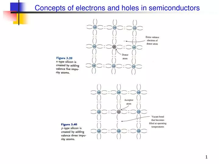
Concepts of electrons and holes in semiconductors. Forward and reverse bias in a p-n junction. Under forward bias the width of the depletion region decreases. Current increases exponentially.

E N D
Forward and reverse bias in a p-n junction • Under forward bias the width of the depletion region decreases. Current increases exponentially. • Under reverse bias the width of the depletion region increases. Very low current flow (leakage current Is)
Chapter 4: Bipolar Junction Transistor 4.1 Basic Operation of the npn Bipolar Junction Transistor Figure 4.1 The npn BJT Basic Operation in the Active Region: We will apply the Shockley equation: • An npn transistor (CE configuration) with variable voltage sources operating in the active region: • VBE ≈ 0.6 V to forward bias the BE junction • VCE >VBE - the base collector junction is reverse biased ……… (4.1) Here, the emission coefficient n = 1 (usually the case for ideal p-n junctions)
Basic Operation in the Active Region – Cont’d Fig. 4.3 • Note: • The current flowing in a BJT is mostly due to electrons moving from the emitter through the base to the collector • Base current consist of two components: (i) holes crossing from the base into the emitter, and (ii) holes recombining with the electrons injected into the base • Usually we desire the base current (i/p current) to be very low First-Order Common-Emitter Characteristics
Factors affecting the Current Gain Note: The BJT can be considered as a current controlled current source. Input current is Ib and output current is Ic. • For designing a BJT with high β the following points should be considered: • Emitter doping should be higher than base doping • - this gives higher gain, since electron current constituting the collector current will be much more than the hole current constituting the base current • The base width should be very small • - reduce base recombination so that most of the electron current from emitter flows to collector • The geometry of the device should allow quick diffusion of electrons to the collector junction, and the electron lifetime in the base should be large • - reduce base recombination current so that most of the electron current from emitter flows to collector
Device Equations – Cont’d From Eq. 4.3 and 4.4 we have: