Download
1 / 33
340 likes | 475 Views
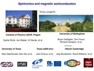
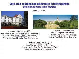
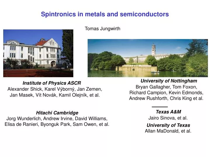
Spintronics in metals and semiconductors. Tom as Jungwirth. Universit y of Nottingham Bryan Gallagher, Tom Foxon, Richard Campion, Kevin Edmonds, Andrew Rushforth, Chris King et al. Institute of Physics ASCR Alexander Shick , Karel Výborný, Jan Zemen,

E N D
Spintronics in metals and semiconductors Tomas Jungwirth University of Nottingham Bryan Gallagher, Tom Foxon, Richard Campion, Kevin Edmonds, Andrew Rushforth, Chris King et al. Institute of Physics ASCR Alexander Shick, Karel Výborný, Jan Zemen, Jan Masek, Vít Novák,Kamil Olejník, et al. Hitachi Cambridge Jorg Wunderlich, Andrew Irvine, David Williams, Elisa de Ranieri, Byonguk Park, Sam Owen, etal. Texas A&M Jairo Sinova, et al. University of Texas Allan MaDonald, et al.
Outline 1. Tunneling anisotropic magnetoresistance in transition metals 2. Ferromagnetism in (Ga,Mn)As and related semiconductors 3. Spintronic transistors
Spintronics: Spin-orbit & exchange interactions nucleus rest frame electron rest frame Thomas precession spin-orbit interaction DOS Coulomb repulsion & Pauli exclusion principle exchange interaction ferromagnetism
Au AMR TMR ~ 1% MR effect ~ 100% MR effect Exchange int.: Spin-orbit int.: magnetic anisotropy TAMR Exchange int.: AFM-FM exchange bias
TAMR in CoPt structures ab intio theory Shick, et al, PRB '06, Park, et al, PRL '08 experiment Park, et al, PRL '08
TAMR in TM structures Consider uncommon TM combinations Mn/W ~100% TAMR Consider both Mn-TM FMs & AFMs Shick, et al, unpublished spontaneous moment magnetic susceptibility spin-orbit coupling exchange-spring rotation of the AFM Scholl et al. PRL ‘04 Proposal for AFM-TAMR: first microelectronic device with active AFM component Shick, et al, unpublished
Outline 1. Tunneling anisotropic magnetoresistance in transition metals 2. Ferromagnetism in (Ga,Mn)As and related semiconductors 3. Spintronic transistors
TM-based semiconducting multiferroic spintronics sensors & memories transistors & logic Magnetic materials spintronic magneto-sensors, memories Semiconductors Ferroelectrics/piezoelectrics transistors, logic, sensitive to doping and electrical gating electro-mechanical transducors, large & persistent el. fields
Ga Mn As Mn Ferromagnetic semiconductors Need true FSs not FM inclusions in SCs GaAs - standard III-V semiconductor Group-II Mn - dilute magnetic moments & holes (Ga,Mn)As - ferromagnetic semiconductor
Ga Mn As Mn GaAs:Mn – extrinsic p-type semiconductor EF spin ~1% Mn << 1% Mn >2% Mn DOS Energy spin onset of ferromagnetism near MIT As-p-like holes localized on Mn acceptors valence band As-p-like holes As-p-like holes FM due to p-d hybridization (Zener local-itinerant kinetic-exchange) Mn-d-like local moments
(Ga,Mn)As synthesis high-T growth • Low-T MBE to avoid precipitation • High enough T to maintain 2D growth • need to optimize T & stoichiometry for each Mn-doping Inevitable formation of interstitial Mn-donors compensating holes and moments need to anneal out optimal-T growth
Interstitial Mn out-diffusion limited by surface-oxide Polyscrystalline 20% shorter bonds O GaMnAs-oxide x-ray photoemission MnI++ GaMnAs Olejnik et al, ‘08 10x shorther annealing with etch Optimizing annealing time & temperature (removing int. Mn & keeping MnGa in place) is essential Rushforth et al, unpublished
Tc limit in (Ga,Mn)As remains open Indiana & California (‘03): “ .. Ohno’s ‘98 Tc=110 K is the fundamental upper limit ..” Yu et al. ‘03 Nottingham & Prague (’08): Tc up to 188 K so far California (‘08): “…Tc =150-165 K independent of xMn>10% contradicting Zener kinetic exchange ...” ? Mack et al. ‘08 “Combinatorial” approach to growth with fixed growth and annealing cond.
Other (III,Mn)V’s DMSs Kudrnovsky et al. PRB 07 Delocalized holes long-range coupl. Weak hybrid. Mean-field but low TcMF InSb d5 Impurity-band holes short-range coupl. Strong hybrid. Large TcMF but low stiffness GaP (Al,Ga,In)(As,P) good candidates, GaAs seems close to the optimal III-V host
Other DMS candidates III = I + II Ga = Li + Zn GaAs and LiZnAs are twin SC (Ga,Mn)As and Li(Zn,Mn)As should be twin ferromagnetic SC • But Mn isovalent in Li(Zn,Mn)As • no Mn concentration limit and self-compensation • possibly both p-type and n-type ferromagnetic SC (Li / Zn stoichiometry) Masek et al. PRL 07
Towards spintronics in (Ga,Mn)As: FM & transport Dilute-moment MS F~ d- Dense-moment MS F<< d- Eu - chalcogenides Broad peak near Tc disappeares with annealing (higher uniformity)??? Critical contribution to resistivity at Tc ~ magnetic susceptibility
(Ga,Mn)As (PragueNottingham) Critical contribution at Tc to d/dT like TM FMs Fe Fisher & Langer ’68 Ni Novak et al., ‘08 d/dT ~ cv F ~ d-
Tc Ni EuCdSe Tc
Ga Mn As Mn p s V Beff Ferromagnetism & strong spin-orbit coupling As-p-like holes Strong SO due to the As p-shell(L=1) character of the top of the valence band Beff Bex + Beff TAMR discovered in (Ga,Mn)As Gold et al. PRL’04
SO couped carries scattering coherently off Coulomb & polarized-magnetic potential of Mn AMR in DMSs MnGa ~ magnetic. only > > sign and magnitude (numerical) consistent with experiment max AMR
Remark: Extraordinary MRs & quantum coherent transport phenomena UCF dirty metal
Outline 1. Tunneling anisotropic magnetoresistance in transition metals 2. Ferromagnetism in (Ga,Mn)As and related semiconductors 3. Spintronic transistors
Gating of the highly doped (Ga,Mn)As: p-n junction FET p-n junction depletion estimates ~25% depletion feasible at low voltages Olejnik et al., ‘08
AMR Increasing and decreasing AMR, Tc, coercivity with depletion
Persistent variations of magnetic properties with ferroelectric gates Stolichnov et al., Nat. Mat.‘08
Electro-mechanical gating with piezo-stressors Strain & SO Rushforth et al., ‘08 Electrically controlled magnetic anisotropies
(Ga,Mn)As spintronic single-electron transistor Wunderlich et al. PRL ‘06 Huge, gatable, and hysteretic MR Single-electron transistor Two "gates": electric and magnetic
AMR nature of the effect Coulomb blockade AMR normal AMR
Single-electron charging energy controlled by Vg and M M [010] [110] F Q VD [100] Source Drain [110] [010] Gate VG Q0 Q0 e2/2C magnetic electric & SO-coupling (M) control of Coulomb blockade oscillations
Theory confirms chemical potential anisotropies in (Ga,Mn)As & predicts CBAMR in SO-coupled room-Tc metal FMs • CBAMR if change of |(M)| ~ e2/2C • In our (Ga,Mn)As ~ meV (~ 10 Kelvin) • In room-T ferromagnet change of |(M)|~100K • Room-T conventional SET • (e2/2C>300K) possible
V DD V V A B V B V A 1 Nonvolatile programmable logic 0 ON OFF Variant p- or n-type FET-like transistor in one single nano-sized CBAMR device 1 0 ON OFF 1 1 0 0 0 1 1 0 OFF ON OFF ON ON OFF ON Vout 0 1 1 1 0 0 1 A B Vout 0 0 0 1 0 1 0 1 1 1 1 1 1 OFF ON OFF 1 1 0 0 “OR” OFF ON OFF ON
V DD V V A B V B V A 1 Nonvolatile programmable logic 0 ON OFF Variant p- or n-type FET-like transistor in one single nano-sized CBAMR device 1 0 ON OFF Vout A B Vout 0 0 0 1 0 1 0 1 1 1 1 1 “OR”
Device design Physics of SO & exchange Materials Chemical potential CBAMR TM FMs, MnAs, MnSb SET (III,Mn)V, I(II,Mn)V DMSs Tunneling DOS TAMR Tunneling device Mn-based TM FMs&AFMs Group velocity & lifetime AMR TM FMs Resistor