Download

1 / 24
240 likes | 352 Views
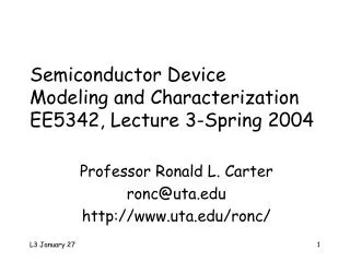
Semiconductor Device Modeling and Characterization – EE5342 Lecture 34 – Spring 2011. Professor Ronald L. Carter ronc@uta.edu http://www.uta.edu/ronc/. The npn Gummel-Poon Static Model. C. R C. I CC - I EC = IS ( exp(v BE /NFV t - exp(v BC /NRV t )/Q B. I BR. B. R BB. I LC.

E N D
Semiconductor Device Modeling and Characterization – EE5342 Lecture 34 – Spring 2011 Professor Ronald L. Carter ronc@uta.edu http://www.uta.edu/ronc/
The npn Gummel-Poon Static Model C RC ICC -IEC = IS(exp(vBE/NFVt - exp(vBC/NRVt)/QB IBR B RBB ILC B’ IBF ILE RE E
IBF = ISexpf(vBE/NFVt)/BF ILE = ISEexpf(vBE/NEVt) IBR = ISexpf(vBC/NRVt)/BR ILC = ISCexpf(vBC/NCVt) QB = (1 + vBC/VAF + vBE/VAR ) {½ + [¼ + (BFIBF/IKF + BRIBR/IKR)]1/2 } Gummel Poon npnModel Equations
fms (V) Fig 10.15* NB (cm-3) Typical fms values
Flat band with oxidecharge (approx. scale) Al SiO2 p-Si +<--Vox-->- q(Vox) Ec,Ox q(ffp-cox) Ex q(fm-cox) Eg,ox~8eV Ec EFm EFi EFp q(VFB) Ev VFB= VG-VB, when Si bands are flat Ev
Inversion for p-SiVgate>VTh>VFB Vgate> VFB EOx,x> 0 e- e- e- e- e- Acceptors Depl Reg Vsub = 0
Approximation concept“Onset of Strong Inv” • OSI = Onset of Strong Inversion occurs when ns = Na = ppo and VG= VTh • Assume ns = 0 for VG< VTh • Assume xdepl = xd,max for VG = VTh and it doesn’t increase for VG > VTh • Cd,min = eSi/xd,max for VG > VTh • Assume ns > 0 for VG > VTh
Fig 10.9* qfp 2q|fp| xd,max MOS Bands at OSIp-substr = n-channel
Computing the D.R. W and Q at O.S.I. Ex Emax x
Fully biased n-MOScapacitor VG Channel if VG > VT VS VD EOx,x> 0 e- e- e- e- e- e- n+ n+ p-substrate Vsub=VB Depl Reg Acceptors y 0 L
MOS energy bands atSi surface for n-channel Fig 8.10**
Ex Emax x Computing the D.R. W and Q at O.S.I.
Q’d,max and xd,max forbiased MOS capacitor Fig 8.11** xd,max (mm)
n-channel VT forVC = VB = 0 Fig 10.20*
References * Semiconductor Physics & Devices, by Donald A. Neamen, Irwin, Chicago, 1997. **Device Electronics for Integrated Circuits, 2nd ed., by Richard S. Muller and Theodore I. Kamins, John Wiley and Sons, New York, 1986