Download
1 / 28
820 likes | 1.5k Views
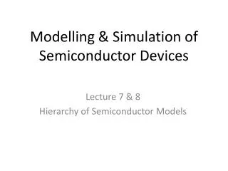
Modelling & Simulation of Semiconductor Devices. Lecture 5 & 6 Basics of Device Modelling Approaches. Device Modeling.

E N D
Modelling & Simulation of Semiconductor Devices Lecture 5 & 6 Basics of Device Modelling Approaches
Device Modeling • It is extremely important to have a valid device modeling & simulation design prior to the device fabrication b/c technology & design iteration are expensive and post fabrication tuning is not a fun. • Modern device designing is very complex, so it is difficult to predict performance characteristics of device without accurate computer models. • Device modeling actually describes the principal methods of representing and analyzing devices. • Device modeling is useful in device design, production control and performance analysis.
Device Modeling • The utmost purpose of any device modeling is to • Cuts Cost (economical) • Cuts development time (faster manufacturing) • Accurate designing • “cutting edge” concept (reduced size). • Minimize system complexities
Device Modelling Classification • Diode device Modeling • Transistor deviceModeling • Semiconductor device Modeling (ICs)
Diode device Modeling • Diode Modeling: refers to the mathematical models used to approximate the actual behavior of real diodes to enable calculations and circuit analysis. • diode's V-I curve is nonlinear • This nonlinearity complicates calculations in circuits involving diodes, so simpler models are often required.
Diode device Modeling • Diode Modeling may be categorized as • Large signal diode modeling (Non-linear): deals with any ACTIVEcomponents. • Shockley diode model • Diode-resistor model • Large signal diode modeling is based on either • Graphical modeling method • Piecewise linear (PWL) modeling • Mathematically idealized diode Modeling • small signal diode modeling (Linear):deals with any PASSIVE components. • Resistance, Capacitance.
Graphical modeling method • Graphical analysis is a simple way to derive a numerical solution to the transcendental equations describing the diode. • As with most graphical methods, it has the advantage of easy visualization. • By plotting the V-I curves, it is possible to obtain an approximate solution to any arbitrary degree of accuracy. • This method plots the two current-voltage equations on a graph and the point of intersection of the two curves satisfies both equations, giving the value of the current flowing through the circuit and the voltage across the diode. • Graphical method is often time consuming and is impractical for complex circuits . A transcendental function is a function that does not satisfy a polynomial equation whose coefficients are themselves polynomials, in contrast to an algebraic function, which does satisfy such an equation.
Piecewise linearmodeling • Piecewise linear (PWL) modelingtakes a function f(t) and breaks it into several linear segments. • The graph shows how a curve can be approximated by three linear segments, forming a three-segment PWL model. • PWL method is used to approximate the diode characteristic curve into linear segments. • This enables us to substitute the real diode for an ideal diode, a voltage source and a resistor. • The figure shows a real diode V-I curve being approximated by a two segment PWL model. • Typically the sloped line segment would be chosen tangent to the diode curve at the Q-point. • Then the slope of this line is given by the reciprocal of the small-signal resistance of the diode at the Q-point. piecewise linear approximation of a curve A piecewise linear approximation of the diode characteristic.
Mathematically idealized diode • Let us consider a mathematically idealized diode. • In such an ideal diode, if the diode is reverse biased, the current flowing through it is zero. • This ideal diode starts conducting at 0 V and for any positive voltage an infinite current flows and the diode acts like a short circuit. • The I-V characteristics of an ideal diode are shown. I-V characteristic of an ideal diode
Ideal diode in series with voltage source • Consider the case when we add a voltage source in series with the diode as shown . • When forward biased, ideal diode is simply a short circuit and when reverse biased, an open circuit. • If the anode of the diode is connected to 0 V, voltage at the cathode will be at Vt and the potential at the cathode will be greater than the potential at the anode and the diode will be reverse biased. • In order to get the diode to conduct, voltage at the anode will need to be taken to Vt. • This circuit approximates the cut-in voltage present in real diodes. • The combined I-V characteristic of this circuit is shown . Ideal diode with a series voltage source I-V characteristic of and ideal diode with a series voltage source
Diode with voltage source & current-limiting resistor • The last thing needed is a resistor to limit the current, as shown with the I-V characteristic. • The real diode now can be replaced with the combined ideal diode, voltage source and resistor and the circuit then is modeled using just linear elements. • If the sloped-line segment is tangent to the real diode curve at the Q-point, this approximate circuit has the same small-signal circuit at the Q-point as the real diode. Ideal diode with a series voltage source and resistor I-V characteristic of an ideal diode with a series voltage source and resistor
Transistor device Modeling • Transistors are simple devices with complicated behavior. • In order to ensure the reliable operation of circuits employing transistors, it is necessary to scientifically model the physical phenomena observed in their operation using transistor models. • There exists a variety of different models that range in complexity and in purpose. • Transistor models divide into two major groups: • Models for device design • Models for circuit design
Models for device design • Modern transistor has an internal structure that exploits complex physical mechanisms. • Device design requires a detailed understanding of how device manufacturing processes carried like Ion implantation, Impurity diffusion, Oxide growth, Annealing, Etching affect device behavior. • Process models simulate the manufacturing steps and provide a microscopic description of device "geometry" to the device simulator. • By "geometry" is meant not only readily identified geometrical features such as whether the gate is planar or wrap-around, or whether the source and drain is altered or not but also details inside the structure, such as the doping profiles after completion of device processing. • Physical processes in the device determine its electrical behavior in a variety of circumstances: • DC current-voltage behavior, • transient behavior (both large-signal and small-signal), • Internal variation in device response.
Models for circuit design (compact models) • Transistor models are used for almost all modern electronic design work. • Analog circuit simulators such as SPICE (Simulation Program with Integrated Circuit Emphasis) use models to predict the behavior of a design. • LT SPICE is getting popularity too. • Most design work is related to IC designs which have a very large tool cost, primarily for the photo masks used to create the devices, and there is a large economic incentive to get the design working without any iterations. • Device models must include effect of various parameters on design like: • Width & length • Interdigitation • Proximity to other devices • Transient and DC current-voltage characteristics • Parasitic device capacitance • Resistance and inductance • Time delays • Temperature effects
Transistor – Large signal nonlinear models • Large signal transistor models (non-linear models) fall into three main types. • Physical models • Empirical models • Tabular models
Physical models • These are models based upon device physics, which relies on the approximate modeling of physical phenomena within a transistor. • Parameters within these models are based upon physical properties such as • Oxide thicknesses, Substrate doping concentrations, Carrier mobility, etc.
Empirical models • Empirical models are based upon curve fitting, subjected to the parameter and values which can fit describe the operation of the device (transistor). • Unlike a physical model, empirical model parameters are not based fundamentals, they mostly depends on the fitting procedure used to find them. • Fitting procedure is key to success of these models if they are to be used to extrapolate to designs lying outside the range of data to which the models were originally fitted. Empirical model of carrier scattering on ionized impurity
Tabular models • Tabular models are based on look-up table (LUT) form, by considering effect of one parameter to the other. • Effect of parasitic components on drain current • These values are indexed in reference to their corresponding bias voltage combinations. • Thus, model accuracy is increased by inclusion of additional data points within the table. • Limitation of these models is that they work best for designs that use devices within the table (interpolation) and are unreliable for devices outside the table (extrapolation).
Transistor – Small-signal linear models • Small-signal or linear models are used to evaluate stability, gain, noise and bandwidth. • A small-signal model is generated by taking derivatives of the current-voltage curves about a bias point or Q-point. • As long as the signal is small relative to the nonlinearity of the device, the derivatives do not vary significantly, and can be treated as standard linear circuit elements. • Advantage of small signal models is that they can be solved directly, while large signal nonlinear models are generally solved iteratively, with possible convergence or stability issues. • By simplification to a linear model, the whole apparatus for solving linear equations becomes available, for example, simultaneous equations, determinants, and matrix theory etc.
Small-signal parameters • A transistor’s parameters represent its electrical properties. • Engineers employ transistor parameters in production-line testing and in circuit design. • A group of a transistor’s parameters sufficient to predict circuit gain, input impedance, and output impedance are components in its small-signal model. • Parameters used in small-signal circuits (two ports) adopt names related to the names of these circuits such as • Transmission parameters (T-parameters), • Hybrid-parameters (h-parameters), • Impedance parameters (z-parameters), • Admittance parameters (y-parameters), and • Scattering parameters (S-parameters). • These parameters all can be evaluated using measured scattering parameter data. • Scattering parameters (S parameters) can be measured for a transistor at a given bias point with a vector network analyzer.
Semiconductor device modeling • Semiconductor device modeling creates models for the behavior of the electrical devices based on fundamental physics, such as the doping profiles of the devices. • The intent of IC fabrication is to produce a wafer with specific electrical & mechanical characteristics, usually in the form of electronic circuits or chips, via some number of processing transformations.
Why need semiconductor modeling? • semiconductor modeling is based on a computational modeling mechanism, which is theevaluation & optimization of various design, without resorting to costly and time-consuming trial fabrication and measurement steps. • It may also include the creation of compact models (such as the SPICE(Simulation Program with Integrated Circuit Emphasis) transistor models, which try to capture the electrical behavior of such devices but do not generally derive them from the underlying physics. • Provides valuable insight into important physical quantities. • Shortened development cycles. • Reduced cost. • Increased quality and reliability of final products. • A important field of computational modeling related to semiconductor manufacturing belongs to process modeling.
Semiconductor device models • Semiconductor device models can be considered in two broad categories • Physical device models • Equivalent circuit models. • Physical device models: attempt to incorporate the physics of device operation. • Equivalent circuit models: are based on electrical circuit analogies representing the electrical behavior.
Physical device models • Physical device models can provide greater insight into the detailed operation andoperating conditions of semiconductor devices, but usually based on a lengthy analysis. • Dependent on numerical techniques implemented on computers. • Physical device models are solved using either bulk carrier transport equations(the semiconductor equations), solutions to the Boltzmann transport equation or quantum transport concepts. • Bulk transport solutions have satisfied most device models • Boltzmann and quantum transport solutions have provided a strong insight into the detailed device physics. • The understanding of material properties, physical boundary conditions (such as surface physics, contact properties and device geometry) and device-circuit interaction are steadily improving, allowing more intricate models to be developed.
Equivalent circuit models • Equivalent circuit modelsapproach is generally limited in its applicability because of the DC bias, frequency dependence and the non-linear behavior of most devices with respect to signal level. • The principal advantage of this technique is that it is easy to implement and analyze.
Equivalent circuit models BJT Equivalent Circuit th rough diode Equivalent Circuit Model: NPN BJT Small signal
To download this lecture visit http://imtiazhussainkalwar.weebly.com/ End of Lectures 5-6