Download
1 / 16
190 likes | 493 Views
LOW POWER MICROCONTROLLER DESIGN BY USING UPF. Borisav Jovanović , Milunka Damnjanović , Faculty of Electronic Engineering Niš. THE CONTENT OF PRESENTATION. Introduction Power managing strategy Power supply network design of 8051 microcontroller block Implementation results Conclusion.

E N D
LOW POWER MICROCONTROLLER DESIGN BY USING UPF BorisavJovanović, MilunkaDamnjanović, Faculty of Electronic Engineering Niš
THE CONTENT OF PRESENTATION • Introduction • Power managing strategy • Power supply network design of 8051 microcontroller block • Implementation results • Conclusion
1. INTRODUCTION Power dissipation is today one of the key parts of design specifications of the System-on-Chip (SoCs), complex analog and digital systems integrated on the single IC. In this paper, low power design techniques which have an emphasis on modern standard cell process technologies are presented and investigated. Special attention is put on leakage power minimization. As an example, 8051 microcontroller block is used.
Leakage power: 2. POWER MANAGING STRATEGY Figure 1. Impact of technology scaling on leakage power share in the total power for SoC design
The leakage elimination techniques : • voltage scaling, • multi voltage design, • multi threshold standard cell libraries, • power gating. Reducing the supply voltage The leakage power reduces linearly with the decreasing of supply voltage Vdd Multiple threshold voltage cells • The digital logic cells are present usually in two forms: • High VTH cell library have lower leakage currents and therefore consume less power but have larger delays. • Low VTH cells have the good timing characteristics but consume more power then high VTH.
Power shutdown Power gating is done by placing one PMOS transistor and one NMOS transistor in series with the transistors of each block to create virtual ground and virtual power supply Figure 2. MTCMOS switches for power shutdown Isolation cells are used to save CMOS logic levels on the power gated outputs Figure 3. Isolation cell and relevant signals
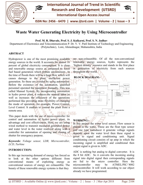
Figure 4. State retention flip-flop cell and relevant signals State retention cells are used to save the information while power down state The SRPG cell has main power supply input (VDD) for active operation when it can change its state. Beside, the cell has an extra power supply input, called retention voltage (VRET) for state retention purpose.
The Unified Power Format (UPF) is new standard that enables the electronic systems to be designed with a power as a key consideration. • The UPF information covers many issues : • how the core of chip is divided into power domains • how the power supply network is created to supply power domain areas • how individual supply net behaves with respect to one another, • how the logic functionality is extended to support dynamic power switching within domain Figure 5. Design flow supported by UPF
3. POWER SUPPLY NETWORK DESIGN OF 8051 BLOCK The instruction set contains 255 instructions. Data path is pipelined and one-byte instructions are executed in a single clock cycle. Chip consists of MCU core, memory blocks peripheral units • The on-chip peripherals: • three digital input/output parallel ports (Port0, Port1, Port2); • LCD driver (up to 168 pixels LCD display) • communication modules –2 USARTs and I2C • three timer/counter circuits (TC0, TC1 and TC2). • Memories: • Program memory (on-chip 8kB SRAM block), • External data memory (XRAM - on-chip 2kB SRAM block), • Internal data memory (IRAM - 256 Dual port RAM and Special Function Registers)
Power domains: • TOP • MCU core, • peripherals • and memories. Figure 6. The block diagram of chip’s power domains create_power_domain TOP create_power_domain CORE -elements U_CORE create_power_domain PER -elements U_Per create_power_domain MEM -elements {U_CORE/ram/U1 U_CORE/ram/U9 U_CORE/rom/U2/msbg U_CORE/rom/U2/lsbg U_CORE/core51/t51_ram/U20 U_CORE/core51/t51_ram/U1 } Figure 7. The UPF code for specifying the domains
create_supply_port VDD create_supply_net VDD -domain TOP create_supply_net VDD -domain CORE -reuse create_supply_net VDD -domain PER -reuse create_supply_net VDD -domain MEM -reuse connect_supply_net VDD -ports VDD create_supply_port VSS create_supply_net VSS -domain TOP create_supply_net VSS -domain CORE -reuse create_supply_net VSS -domain PER -reuse create_supply_net VSS -domain MEM -reuse connect_supply_net VSS -ports VSS create_supply_net VDDCOR -domain CORE create_supply_net VDDPER -domain PER set_domain_supply_net TOP -primary_power_net VDD -primary_ground_net VSS set_domain_supply_net CORE -primary_power_net VDDCOR -primary_ground_net VSS set_domain_supply_net PER -primary_power_net VDDPER -primary_ground_net VSS set_domain_supply_net MEM -primary_power_net VDD -primary_ground_net VSS Each voltage domain has its own power supply net which is derived from the main net VDD. The supply VDDCOR was used to supply the microcontroller core. Net VDDPER is chosen for peripheral‘s supply. Figure 8. The UPF code for creating the power supply nets
create_power_switch CORE_sw \ -domain CORE \ -input_supply_port {in VDD} \ -output_supply_port {out VDDCOR} \ -control_port {Power_CORE U_PCTL/Power_CORE} \ -on_state {state2003 in {Power_CORE}} set_isolation CORE_iso_out \ -domain CORE \ -isolation_power_net VDD -isolation_ground_net VSS \ -clamp_value 1 \ -applies_to outputs set_isolation_control CORE_iso_out \ -domain CORE \ -isolation_signal U_PCTL/ISO_CORE \ -isolation_sense high \ -location parent Figure 9. The UPF part of code for specifying switches
The operation of Power Management Unit In Standby mode, the microcontroller’s core is switched off from power supply while the peripherals and memories were kept powered. Power management unit turns off the VDDCORE while keeping the VDDPER and VDDMEM. The memories are powered to retain the program code and data. The peripherals are kept powered to enable the wake up sequence and MCU safe returning into Active mode. • While bringing the chip into the Standby mode, the Power management unit performs several operations: • issues the reset signal for MCU core. • activates the isolation cells located on the interface between MCU core and the neighboring blocks • activates the Sleep signal to activate MTCMOS cells. The Sleep signal switches off the MCU core from VDD.
4. IMPLEMENTATION RESULTS The chip was implemented in Synopsys 90nm, working at 1.2V, implemented by Synopsys tools (Design Compiler for synthesis and IC Compiler for floor- planning, placement and routing). The power consumption of MCU was simulated to be 0.68mW at 3.75MHz. The leakage power of 0.41mW forms almost 60% of total power. The dynamic power of power optimized design is only 0.27mW. Paverage=0.41+0.07*f Figure 10.Microcontroller’s power dissipation function Figure 11. Impact of technology scaling
The obtained block area is 1.485 mm2 Figure 12. The MCU layout in 90nm technology The leakage power became 0.1mW instead of 0.4mW that was before use of the leakage reduction techniques. The static power reduction achieved in Standby mode is 75% comparing to the design which did not use the benefits of power gating.
The leakage minimization techniques implemented in MCU core are: supply voltage reduction, utilization of multi-VTH libraries and power gating. The leakage power reduction in 90nm technology achieved by power saving modes is 75%. The leakage power became 0.1mW instead of 0.4mW that was before use of the leakage reduction techniques. The main objective, which was to realize power efficient design, was fully reached. 5. CONCLUSION