Download
1 / 68
960 likes | 2.07k Views
Chapter 16 Frequency Response. Microelectronic Circuit Design Richard C. Jaeger Travis N. Blalock. Chapter Goals. Review transfer function analysis and dominant-pole approximations of amplifier transfer functions. Learn partition of ac circuits into low and high-frequency equivalents.

E N D
Chapter 16Frequency Response Microelectronic Circuit Design Richard C. Jaeger Travis N. Blalock Microelectronic Circuit Design, 3E McGraw-Hill
Chapter Goals • Review transfer function analysis and dominant-pole approximations of amplifier transfer functions. • Learn partition of ac circuits into low and high-frequency equivalents. • Learn the short-circuit time constant method to estimate upper and lower cutoff frequencies. • Develop bipolar and MOS small-signal models with device capacitances. • Study unity-gain bandwidth product limitations of BJTs and MOSFETs. • Develop expressions for upper cutoff frequency of inverting, non-inverting and follower configurations. • Explore high-frequency limitations of single and multiple transistor circuits. Microelectronic Circuit Design, 3E McGraw-Hill
Chapter Goals (contd.) • Understand Miller effect and design of op amp frequency compensation. • Develop relationship between op amp unity-gain frequency and slew rate. • Understand use of tuned circuits to design high-Q band-pass amplifiers. • Understand concept of mixing and explore basic mixer circuits. • Study application of Gilbert multiplier as balanced modulator and mixer. Microelectronic Circuit Design, 3E McGraw-Hill
Transfer Function Analysis for ,i =1…l Amid is midband gain between upper and lower cutoff frequencies. for ,j =1…k Microelectronic Circuit Design, 3E McGraw-Hill
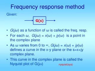
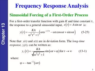
Low-Frequency Response Pole wP2 is called the dominant low-frequency pole (> all other poles) and zeros are at frequencies low enough to not affect wL. If there is no dominant pole at low frequencies, poles and zeros interact to determine wL. Pole wL > all other pole and zero frequencies In general, for n poles and n zeros, For s=jw, at wL, Microelectronic Circuit Design, 3E McGraw-Hill
Low-Frequency Response Microelectronic Circuit Design, 3E McGraw-Hill
Transfer Function Analysis and Dominant Pole Approximation Example • Problem: Find midband gain, FL(s) and fL for • Analysis: Rearranging the given transfer function to get it in standard form, Now, and Zeros are at s=0 and s =-100. Poles are at s= -10, s=-1000 All pole and zero frequencies are low and separated by at least a decade. Dominant pole is at w=1000 and fL =1000/2p= 159 Hz. For frequencies > a few rad/s: Microelectronic Circuit Design, 3E McGraw-Hill
High-Frequency Response Pole wP3 is called the dominant high-frequency pole (< all other poles). If there is no dominant pole at low frequencies, poles and zeros interact to determine wH. Pole wH < all other pole and zero frequencies In general, For s=jw, at wH, Microelectronic Circuit Design, 3E McGraw-Hill
High-Frequency Response Microelectronic Circuit Design, 3E McGraw-Hill
Direct Determination of Low-Frequency Poles and Zeros: C-S Amplifier C3 C2 Microelectronic Circuit Design, 3E McGraw-Hill
Direct Determination of Low-Frequency Poles and Zeros: C-S Amplifier (contd.) The three zero locations are: s = 0, 0, -1/(RS C2). The three pole locations are: Each independent capacitor in the circuit contributes one pole and one zero. Series capacitors C1 and C3 contribute the two zeros at s=0 (dc), blocking propagation of dc signals through the amplifier. The third zero due to parallel combination of C2 and RS occurs at frequency where signal current propagation through MOSFET is blocked (output voltage is zero). Microelectronic Circuit Design, 3E McGraw-Hill
Short-Circuit Time Constant Method to Determine wL • Lower cutoff frequency for a network with n coupling and bypass capacitors is given by: where RiS is resistance at terminals of ith capacitor Ci with all other capacitors replaced by short circuits. Product RiS Ci is short-circuit time constant associated with Ci. Midband gain and upper and lower cutoff frequencies that define bandwidth of amplifier are of more interest than complete transfer function. Microelectronic Circuit Design, 3E McGraw-Hill
Estimate of wL for C-E Amplifier Using SCTC method, for C1, For C2, For C3, Microelectronic Circuit Design, 3E McGraw-Hill
Estimate of wL for C-S Amplifier Using SCTC method, For C1, For C2, For C3, Microelectronic Circuit Design, 3E McGraw-Hill
Estimate of wL for C-B Amplifier Using SCTC method, For C1, For C2, Microelectronic Circuit Design, 3E McGraw-Hill
Estimate of wL for C-G Amplifier Using SCTC method, For C1, For C2, Microelectronic Circuit Design, 3E McGraw-Hill
Estimate of wL for C-C Amplifier Using SCTC method, For C1, For C2, Microelectronic Circuit Design, 3E McGraw-Hill
Estimate of wL for C-D Amplifier Using SCTC method, For C1, For C2, Microelectronic Circuit Design, 3E McGraw-Hill
Frequency-dependent Hybrid-Pi Model for BJT Capacitance between base and emitter terminals is: tF is forward transit-time of the BJT. Cp appears in parallel with rp. As frequency increases, for a given input signal current, impedance of Cp reduces vbe and thus the current in the controlled source at transistor output. Capacitance between base and collector terminals is: Cmo is total collector-base junction capacitance at zero bias, Fjc is its built-in potential. Microelectronic Circuit Design, 3E McGraw-Hill
Unity-gain Frequency of BJT The right-half plane transmission zero wZ = + gm/Cm occurring at high frequency can be neglected. wb = 1/ rp(Cm + Cp ) is the beta-cutoff frequency where and fT = wT /2p is the unity gain bandwidth product. Above fT BJT has no appreciable current gain. Microelectronic Circuit Design, 3E McGraw-Hill
Unity-gain Frequency of BJT (contd.) Current gain is bo = gmrp at low frequencies and has single pole roll-off at frequencies > fb, crossing through unity gain at wT. Magnitude of current gain is 3 dB below its low-frequency value at fb. Microelectronic Circuit Design, 3E McGraw-Hill Chap 17- 21
High-frequency Model of MOSFET Microelectronic Circuit Design, 3E McGraw-Hill Chap 17- 22
Limitations of High-frequency Models • Above 0.3 fT, behavior of simple pi-models begins to deviate significantly from the actual device. • Also, wT depends on operating current as shown and is not constant as assumed. • For given BJT, a collector current ICM exists that yield fTmax. • For FET in saturation, CGS and CGD are independent of Q-point current, so Microelectronic Circuit Design, 3E McGraw-Hill Chap 17- 23
Effect of Base Resistance on Midband Amplifiers To account for base resistance rx is absorbed into equivalent pi model and can be used to transform expressions for C-E, C-C and C-B amplifiers. Base current enters the BJT through external base contact and traverses a high resistance region before entering active area. rx models voltage drop between base contact and active area of the BJT. Microelectronic Circuit Design, 3E McGraw-Hill
Summary of BJT Amplifier Equations with Base Resistance Microelectronic Circuit Design, 3E McGraw-Hill
Single-Pole High Frequency Response Let’s first start with a simple two resistor, one capacitor network. Microelectronic Circuit Design, 3E McGraw-Hill
Single-Pole High Frequency Response (cont.) Substituting s=j2f and using fp=1/(2[R1||R2]C1) This expression has two parts, the midband gain, R2/(R2+R1), and the high frequency characteristic, 1/(1+jf/fp). Microelectronic Circuit Design, 3E McGraw-Hill
Miller Effect We desire to replace Cxy with Ceq to ground. Starting with the definition of small-signal capacitance: Now write an expression for the change in charge for Cxy: We can now find and equivalent capacitance, Ceq: Microelectronic Circuit Design, 3E McGraw-Hill
C-E Amplifier High Frequency Response using Miller Effect First, find the simplifed small-signal model of the C-A amp. Microelectronic Circuit Design, 3E McGraw-Hill
C-E Amplifier High Frequency Response using Miller Effect (cont.) Input gain is found as Terminal gain is Using the Miller effect, we find the equivalent capacitance at the base as: Microelectronic Circuit Design, 3E McGraw-Hill
C-E Amplifier High Frequency Response using Miller Effect (cont.) The total equivalent resistance at the base is The total capacitance and resistance at the collector is Because of interaction through C, the two RC time constants interact, giving rise to a dominant pole Microelectronic Circuit Design, 3E McGraw-Hill
Direct High-Frequency Analysis: C-E Amplifier The small-signal model can be simplified by using Norton source transformation. Microelectronic Circuit Design, 3E McGraw-Hill
Direct High-Frequency Analysis: C-E Amplifier (Pole Determination) From nodal equations for the circuit in frequency domain, High-frequency response is given by 2 poles, one finite zero and one zero at infinity. Finite right-half plane zero, wZ = + gm/Cm > wT can be important in FET amplifiers. For a polynomial s2+sA1+A0 with roots a and b, a =A1 and b=A0/A1. Smallest root that gives first pole limits frequency response and determines wH. Second pole is important in frequency compensation as it can degrade phase margin of feedback amplifiers. Microelectronic Circuit Design, 3E McGraw-Hill
Direct High-Frequency Analysis: C-E Amplifier (Overall Transfer Function) Dominant pole model at high frequencies for C-E amplifier is as shown. Microelectronic Circuit Design, 3E McGraw-Hill
Direct High-Frequency Analysis: C-E Amplifier (Example) • Problem: Find midband gain, poles, zeros and fL. • Given data: Q-point= ( 1.60 mA, 3.00V), fT =500 MHz, bo =100, Cm=0.5 pF, rx =250W, CL =0 • Analysis: gm=40IC =40(0.0016) =64 mS, rp = bo/gm =1.56 kW. Microelectronic Circuit Design, 3E McGraw-Hill
Spice Simulation of Example C-E Amplifier Microelectronic Circuit Design, 3E McGraw-Hill
Estimation of wH using the Open-Circuit Time Constant Method At high frequencies, impedances of coupling and bypass capacitors are small enough to be considered short circuits. Open-circuit time constants associated with impedances of device capacitances are considered instead. where Rio is resistance at terminals of ith capacitor Ci with all other capacitors open-circuited. For a C-E amplifier, assuming CL =0 Microelectronic Circuit Design, 3E McGraw-Hill
High-Frequency Analysis: C-S Amplifier Analysis similar to the C-E case yields the following equations: Microelectronic Circuit Design, 3E McGraw-Hill
C-S Amplifier High Frequency Response with Source Degeneration Resistance First, find the simplifed small-signal model of the C-A amp. Recall that we can define an effective gm to account for the unbypassed source resistance. Microelectronic Circuit Design, 3E McGraw-Hill
C-S Amplifier High Frequency Response with Source Degeneration Resistance (cont.) Input gain is found as Terminal gain is Again, we use the Miller effect to find the equivalent capacitance at the gate as: Microelectronic Circuit Design, 3E McGraw-Hill
C-S Amplifier High Frequency Response with Source Degeneration Resistance (cont.) The total equivalent resistance at the gate is The total capacitance and resistance at the collector is Because of interaction through CGD, the two RC time constants interact, giving rise to the dominant pole: And from previous analysis: Microelectronic Circuit Design, 3E McGraw-Hill
C-E Amplifier with Emitter Degeneration Resistance Analysis similar to the C-S case yields the following equations: Microelectronic Circuit Design, 3E McGraw-Hill
Gain-Bandwidth Trade-offs Using Source/Emitter Degeneration Resistor Adding source resistance to the CS amp caused gain to decrease and dominant pole frequency to increase. However, decreasing the gain also decreased the frequency of the second pole. Increasing the gain of the C-E/C-S stage causes pole-splitting, or increase of the difference in frequency between the first and second poles. Microelectronic Circuit Design, 3E McGraw-Hill
High Frequency Poles for the C-B Amplifier Since C does not couple input and output, input and output poles can be found directly. Microelectronic Circuit Design, 3E McGraw-Hill
High Frequency Poles for the C-G Amplifier Similar to the C-B, since CGD does not couple the input and output, input and output poles can be found directly. Microelectronic Circuit Design, 3E McGraw-Hill
High Frequency Poles for the C-C Amplifier Microelectronic Circuit Design, 3E McGraw-Hill
High Frequency Poles for the C-C Amplifier (cont.) The low impedance at the output makes the input and output time constants relatively well decoupled, leading to two poles. The feed-forward high-frequency path through Cp leads to a zero in the C-C response. Both the zero and the second pole are quite high frequency and are often neglected, although their effect can be significant with large load capacitances. Microelectronic Circuit Design, 3E McGraw-Hill
High Frequency Poles for the C-D Amplifier Similar the the C-C amplifier, the high frequency response is dominated by the first pole due to the low impedance at the output of the C-C amplifier. Microelectronic Circuit Design, 3E McGraw-Hill
Summary of the Upper-Cutoff Frequencies of the Single-Stage Amplifiers (pg.1037) Microelectronic Circuit Design, 3E McGraw-Hill
Frequency Response: Differential Amplifier CEE is total capacitance at emitter node of the differential pair. Differential mode half-circuit is similar to a C-E stage. Bandwidth is determined by the product. As emitter is a virtual ground, CEE has no effect on differential-mode signals. For common-mode signals, at very low frequencies, Transmission zero due to CEE is Microelectronic Circuit Design, 3E McGraw-Hill