Download
1 / 21
210 likes | 391 Views
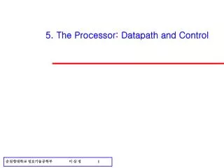
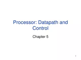
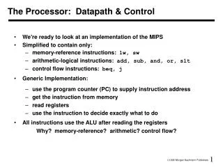
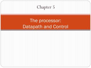
The processor: Datapath and Control. Chapter 5. 0. 35 or 43. 4. rs. rs. rs. rt. rt. rt. rd. address. address. shamt. funct. 31:26. 31:26. 31:26. 25:21. 25:21. 25:21. 20:16. 20:16. 20:16. 15:11. 10:6. 15:0. 15:0. 5:0. Review. R-type. Load/ Store. Branch. opcode.

E N D
The processor:Datapath and Control Chapter 5
0 35 or 43 4 rs rs rs rt rt rt rd address address shamt funct 31:26 31:26 31:26 25:21 25:21 25:21 20:16 20:16 20:16 15:11 10:6 15:0 15:0 5:0 Review R-type Load/Store Branch opcode always read read, except for load write for R-type and load sign-extend and add
Q5.1 • A- Multiplexor (Combinational logic only) • B- Comparator (Combinational logic only) • C- Incrementer/Decrementer (Combinational logic only) • D- Barrel Shifter (Mixed sequential and combinational) • E-Multiplier with shifters and adders (Mixed sequential and combinational) • F-Register (Sequential logic only) • G-Memory (Sequential logic only) • H-ALU (Combinational logic only) • I-Carry look_ahead adder (Combinational logic only) • J-Latch (Sequential logic only) • K-General finite state machine(FSM) (Mixed sequential and combinational)
Q5.2 a.. RegWrite = 0: All R-format instructions, in addition to lw will not work because these instructions will not be able to write their results to the register file. b. ALUop1 = 0: All R-format instructions except subtract will not work correctly because the ALU will perform subtract instead of the required ALU operation. c. ALUop0 = 0:beq instruction will not work because the ALU will perform addition instead of subtraction ,so the branch outcome may be wrong. d. Branch (or PCSrc) = 0: beq will not execute correctly. The branch instruction will always be not taken even when it should be taken. e. MemRead = 0: lw will not execute correctly because it will not be able to read data from memory. f. MemWrite = 0: Sw will not work correctly because it will not be able to writeto the data memory.
Q5.3 a. RegWrite = 1: sw and beq should not write results to the register file. Sw ( beq ) will overwrite a random register with either the store address (branch target) or random data from the memory data read port. b. ALUop0 = 1: lw and sw will not work correctly because they will perform subtraction instead of the addition necessary for address calculation. c. ALUop1 = 1: lw and sw will not work correctly. Lw and sw will perform a random operation depending on the least significant bits of the address field instead of addition operation necessary for address calculation. d. Branch = 1: Instructions other than branches ( beq ) will not work correctly if the ALU Zero signal is raised. An R-format instruction that produces zero output will branch to a random address determined by its least significant 16 bits. e. MemRead = 1: All instructions will work correctly. (Data memory is always read, but memory data is never written to the register file except in the case of lw ). f. MemWrite = 1: Only sw will work correctly. The rest of instructions will store their results in the data memory, while they should not.
Q5.8 ( add instruction jr) A modification to the datapath is necessary to allow the new PC to come from a register (Read data 1 port), and a new signal (e.g., JumpReg) to control it through a multiplexor as shown in previous Figure. A new line should be added to the truth table in Figure 5.18 on page 308 to implement the jr instruction and a new column to produce the JumpReg signal.
Q5.9 ( add instruction sll) A modification to the data path is necessary to feed the shamt field (instruction[10:6]) to the ALU in order to determine the shift amount. The instruction is in R-Format and is controlled according to the first line in Figure 5.18 on page 308. The ALU will identify the sll operation by the ALUop field. Figure 5.13 on page 302 should be modified to recognize the opcode of sll : the third line should be changed to 1X1X0000 0010 (to discriminate the add and sll functions), and a new line, inserted, for example, 1X0X0000 0011 (to define sll by the 0011 operation code).
Q5.10 ( add instruction luirt, constant) This implementation doesn't need a modification to the datapath. We can use the ALU to implement the shift operation. The shift operation can be like the one presented for Exercise 5.9, but will make the shift amount as a constant 16. A new line should be added to the truth table in Figure 5.18 on page 308 to define the new shift function to the function unit. (Remember two things: first, there is no funct field in this command; second, the shift operation is done to the immediate field, not the register input).
Q5.11(l_inc)lw $rt,L($rs)addi $rs,$rs,1 A modification is required for the datapath of Figure 5.17 to perform the autoincrement by adding 4 to the $rs register through an incrementer. Also we need a second write port to the register file because two register writes are required for this instruction. The new write port will be controlled by a new signal, "Write 2", and a data port, "Write data 2." We assume that the Write register 2 identifier is always the same as Read register 1 ( $rs ). This way "Write 2" indicates that there is second write to register file to the register identified by "Read register 1," and the data is fed through Write data 2.
Q5.11(l_inc) A new line should be added to the truth table in Figure 5.18 for the l_inc command as follows: RegDst = 0: First write to $rt . ALUSrc = 1: Address field for address calculation. MemtoReg = 1: Write loaded data from memory. RegWrite = 1: Write loaded data into $rt . MemRead = 1: Data memory read. MemWrite = 0: No memory write required. Branch = 0: Not a branch, output from the PCSrc controlled mux ignored. ALUOp = 00: Address calculation. Write2 = 1: Second register write (to $rs ) .
Q5.12 Why it is not possible to modify the single cycle implementation to implement the Load with increment instruction without modifying the register file ?? This instruction requires two writes to the register file. The only way to implement it is to modify the register file to have two write ports instead of one.