Download
1 / 18
180 likes | 314 Views
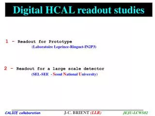
Digital HCAL readout studies. 1 - Readout for Prototype (Laboratoire Leprince-Ringuet-IN2P3). 2 - Readout for a large scale detector (SEL-SEE - S eoul N ational U niversity). CALICE collaboration J-C. BRIENT (LLR) JEJU-LCWS02.

E N D
Digital HCAL readout studies 1 -Readout for Prototype (Laboratoire Leprince-Ringuet-IN2P3) 2 -Readout for a large scale detector (SEL-SEE - Seoul National University) CALICE collaborationJ-C. BRIENT(LLR)JEJU-LCWS02
Studies for the prototype • Design • Test • Construction • of a test set-up for the readout of a digital HCAL WARNING The LLR electronic group working on the project A.Karar, F.Dohou, A.Montgermont CALICE collaborationJ-C. BRIENT(LLR)JEJU-LCWS02
Two examples of RPC as active element by courtesy of Vladimir Ammossov Pad size 1x1 cm2 Pads outside Gas gap thickness 1.2 mm Gas mixture TFE/N2/IB 80/10/10 First measurement Pads inside Efficiency to mip > 98% Signal on 50 W : 1-3 V CALICE collaborationJ-C. BRIENT(LLR)JEJU-LCWS02
Signal output of the RPC Signal (on 50 W) 1 V CALICE collaborationJ-C. BRIENT(LLR)JEJU-LCWS02
Possible readout scheme for a VFE 64 channel chip Requirements Thin PCB (1mm)combining padsandcircuitry Thin packaging, TQFP 1 mm Low power dissipation ~ 1 mW/ch Reading the chips through a token ring CALICE collaborationJ-C. BRIENT(LLR)JEJU-LCWS02
Scheme of the test set-up Test all these idea with readout for cosmic CALICE collaborationJ-C. BRIENT(LLR)JEJU-LCWS02
The test set-up CALICE collaborationJ-C. BRIENT(LLR)JEJU-LCWS02
The FPGA part CALICE collaborationJ-C. BRIENT(LLR)JEJU-LCWS02
The conditioning circuit RPC - FPGA interface The requirements • Current to voltage conversion • Pulse stretching • Digital output (CMOS compatible) • Low input impedance • Overvoltage protection of FPGA • Low power consumption RPC conditioning by current mirror circuit CALICE collaborationJ-C. BRIENT(LLR)JEJU-LCWS02
Results with Current Mirror circuit Output signal VOLT Input signal microseconde CALICE collaborationJ-C. BRIENT(LLR)JEJU-LCWS02
The FPGA-DAQ on PC On MATLAB All readout chain is ready CALICE collaborationJ-C. BRIENT(LLR)JEJU-LCWS02
Design of Readout Electronicsfor digital HCAL on Linear Collider Jaehong Park, Taeyeon Lee, Jinho Sung, Sanghyun Min, Donghwan Lee System Electronics Laboratory School of Electrical Engineering Seoul National University, Seoul, Korea CALICE collaborationJ-C. BRIENT(LLR)JEJU-LCWS02
1cm Pad Detector 64 signals 1cm Control station Readout electronics Control Data 8 x 8 = 64 pads Rise time: 3ns Width: 10~15ns Amplitude: 300~500mV System configuration • Input signal condition • System configuration Typical for RPC CALICE collaborationJ-C. BRIENT(LLR)JEJU-LCWS02
DAC Threshold DAC input Serial link CLK, Selector input CLK Loader WCLK, WEN/ Control Count pulse FF/ Clear LE FIFO 76 x 256 Comparator 1 256 Pad Reset/ 1 1 2 2 Retrieve Serializer RCLK,REN/ Serial_data Q Empty 64 64 EF/ Counted Bunch crossing counter 65 Count pulse Clear 76 Readout Electronics Design • Functional Block Diagram of Readout FPGA DAC Connector Comparators CALICE collaborationJ-C. BRIENT(LLR)JEJU-LCWS02
Command: RESET Command: LOAD CFG DAC DATA MASK DATA Update DAC Command: SET DAC Lower 8bit Upper 2bit Simulation Results of FPGA • Load Dead pixel configuration • Set DAC
Command: MEASURE Measuring Process Command: RETRIEVE Bunch Cross Counter 12bit Comparator Data 64bit Simulation Results of FPGA • Measure • Retrieve
Test Circuit Design • Test Circuit • Check out the functions of Readout Electronics • Test circuit size: 9x9 cm2 FPGA DAC Connector Comparators Component side Solder side CALICE collaborationJ-C. BRIENT(LLR)JEJU-LCWS02
Conclusion All the pieces of the puzzle have been Designed Built Tested FPGA with in front, . aCurrent Mirror circuit (LLR) or ADC+discriminator (SELSEE-SNU) We are ready to read the prototype very soon for a RPC-type signal At least, one conclusionNOW The possibility to design a thin, simple, cheap electronic readout for the digital HCAL, has been demonstrated CALICE collaborationJ-C. BRIENT(LLR)JEJU-LCWS02