Download
1 / 23
230 likes | 341 Views
This report presents the technical status and progress for the HCAL Trigger Readout system. It highlights the principal functions involved in processing front-end data during physics runs, synchronization of optical links, and the extraction of Level 1 trigger information. Key areas include data validation, transmission processes, and calibration processing of various data types. The report discusses recent design changes, testing results, and modifications to enhance reliability, including improvements in board manufacturing, assembly quality, and signal routing, aiming to optimize performance and reduce production risks.

E N D
HCAL Trigger Readout • Technical Status and Progress Report • D. Baden, T. Grassi • http://www.physics.umd.edu/hep/bu_oct_2002.pdf
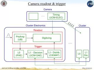
SBS CLK D C C CAL REGIONAL TRIGGER H T R H T R H T R 16 bits @ 80 MHz TTC 32 bits @ 40 MHz QIE CCA GOL QIE QIE CCA QIE GOL QIE CCA QIE FE/DAQ Electronics S-Link: 64 bits @ 25 MHz Trigger Primitives READ-OUT Crate Rack CPU 12 HTRs per Readout Crate, 2 DCC FRONT-END RBX Readout Box (On detector) HPD Shield Wall Fibers at 1.6 Gb/s 3 QIE-channels per fiber FE MODULE
Trigger Readout Principal Functions • Receive front-end data for physics running • Synchronize optical links • Data validation and linearization • Extract Level 1 trigger info, transmit to Level 1 at 40 MHz • Pipeline data, wait for Level 1 accept • Upon receiving L1A: • Zero suppress, format, and transmit to the concentrator • NB: DAQ-Data in QIE-format (non-linear) no filter necessary anyway • Calibration processing and buffering of: • Radioactive source calibration data • Laser/LED calibration data • Support a VME data spy monitoring
“BIT3” board Slow monitoring Commercial VME/PCI Interface to CPU FanOut board Takes TTC stream in Clone and Fanout timing signals HTR (HCALTrigger and Readout) board Spy output over VME FE-Fiber input TPG output (SLBs) to CRT DAQ/TP Data output to DCC DCC (Data Concentrator Card) board Input from HTRs Spy output Output to DAQ Readout VME Crate Front End Electronics TTC fiber Fiber 1.6 Gb/s F a n O u t VME CRATE B I T 3 H TR H T R H T R H T R D C C ... D C C 20m Copper 1.2 Gb/s DAQ Calorimeter Regional Trigger
“Old” HTR Design (Summer 2002) • Board organized around 2 identical sets of circuitry: • Optical inputs • 1.6 GHz, 8B/10B frames, 3ch/link • Dual LC detectors and drivers • TI TLK2501 Deserializers • Crystal RefClk • TTC 80MHz backup • Xilinx Virtex FPGA XCV1000E • 24 channels each • TPG signals • Sent to SLB over backplane, LVDS • SLBs mounted 6 to a transition board • Level 1 accept output to DCC • LVDS output • VME • Altera FPGA and firmware OLD DESIGN
HTR Functional Experience • What was tested: • VME fully tested and working • Some changes necessary to conform to CMS VME standards • Optical links and synchronization • No indication of any problems. Big success here – was a real worry • LVDS to DCC • Tested, working (Will change cable/connector to Cat 6/RJ45) • Fanout of timing signals on two Cat5 cables • Plan to change to a single Cat6 or Cat7 cable (very low cross-talk) • Firmware – full tests of: • Pipeline and L1A triggering capability • In-line histogramming for source calibration • TTCrx • Not working at all (4 bad on 4 tested). • What was not tested: Anything to do with TPG
HTR Board Experience • Produced ~12 boards • Several bare boards were delivered warped • Many opens under FPGA after assembly (~9 boards) • Some fixed after reflow (a few) • Some worse after reflow (shorts) • X-rayed a few boards, sometimes inconclusive • Some opens on VME side • Non BGA FPGA, indicates bad vias • Few other various open circuits • Finally got ~8 boards to “work” • Questionable reliability
Resulting Modifications • Change board from using white-tin to gold traces • This process was sold to us by the board maker. Our mistake. • Used only for very high volume, cost competitive products, very difficult and expensive to control. • Gold is flatter and not very much more expensive (~$50/board), better for FPGAs • Change assembly house • Insufficient Quality Control on current assembler – they are fired. • We visited 2 high-end assemblers • Modern Machines • Step up and step down oven temp control. • In-line X-ray for BGA QC • Manufacturability Review • Add stiffeners to HTRS • Flexability of 9U VME boards was underestimated • Worry: fine-line BGA (FBGA) can pop connections • Change from FBGA (1.0 mm pitch) to BGA (1.27 mm pitch) • No additional expense, plenty of available real estate, no need to push • Full JTAG capabilities added • Will help with debugging • By making these changes… • We have profited from the summer • We have reduced our production risk considerably
HTR Design Changes • SLB transition board issues: • Worries about so many LVDS signals over backplane for old design • Routing is too complicated • Many signals going to same backplane location • Requires multi-layer routing with many vias • TPG cables very thick • Mechanical issues are very worrisome • SLB changes needed (e.g. height reduced after ECAL redesign…) • Solution: move SLB’s to HTR motherboard • Benefits: • Mechanically attach SLB’s to HTR front panel for mechanical stability • Eases routing requirements, reduces board and assembly risks, cheaper too • Change from Xilinx VirtexE to Virtex2 • More resources, block ram, hardware multipliers • Big cost reduction (save $300k) • More modern chip for long-term maintenance • Clock synchronization • Decouple “80MHz” crystal from FPGA system clock • Will allow us to use crystal to maintain synchronization of serdes • This gives us 2 solutions for our “40ps” jitter requirement issue
LVDS LVDS LC LC LC LC LC LC LC LC SLB SLB SLB SLB SLB SLB New HTR Conceptual Design Fibers 8-way P1 TI TI 8-way TI FPGA Xilinx XC2V to DCC VME FPGA TI TI P2 TI TI TI TI TI TI to Level 1 Cal Trigger FPGA Xilinx XC2V TI TI No P3! TI TI TI
HTR Cost Issues • Optical parts • LC receivers quote went up from $80 to $140 • $640/HTR board, $155k total goes up to $270k • We just learned this. Rob is working on them. • Would probably be cost effective now to go with mass terminated receivers (PAROLI) • But would involve board layout changes, will effect schedule, est ~2 months • FPGA • Virtex2 2000 ($472 each, $944/board) current choice ($300k savings), but… • HCAL sections where there is no summing means more LUTs, more resources. • XC2V2000 is just only large enough • VIrtex2 3000 ($743 each, $1486/board) works, pin compatible • Cost increase is $130k total. • Can be minimized by only building HTRs with 3000 part for those sections of HCAL where there is no summing • Reduces cost increase to ~$30k if only HB has the larger chips • Obvious down side is that we would have 2 types of HTRs • Means that HB cards can be used anywhere but not vice versa
HTR Cost Issues (cont) • SLB cost increases • Previous costs were ~$100/SLB • We need 575 total, or $60k in previous budgets • Current estimates from Dasilva: • 292 CHF parts, 100 CHF assembly/testing = $250/SLB • New estimates mean increase to $144k ($86k increase) • We are investigating whether we can buy the parts and assemble them here • SLB transition card • Abandoned (see above) • Cost savings of $66k • TPG cables • Wesley private communication cost estimate was ~$100/cable (2 yrs ago) • Current estimate: $200/cable, $150/connectors and assembly • Increases our cost from $52k to $182k • We are going to have to do our own cost estimates. • Dasilva is testing a much cheaper cable • It is important to push Wesley to decrease the spec from 20m to 10m • Can use smaller cable, saves money, and saves us 2 clock ticks in L1 latency
Cost/Maintenance Issues • Currently, we have 10% spares in the budget. • Optical parts will surely be difficult to get in >3 years • Failure rate is expected to be low but… • If we need more…we propose we buy an extra 10% spares • Additional $15k • FPGAs will probably be ok for 5 years but will be more and more difficult to get, and more and more expensive. • TI serdes will probably be difficult to replace. • $200/HTR board, $46k total • We should buy an extra 10% of these and let them sit in a drawer • PCBs • We propose to build 20% spare PCBs but only stuff 10% • Gives us some breathing room in case of future disasters.
TTCrx TTCrx Clocking Changes OLD SCHEMATIC OLD SCHEMATIC Cat 5 quad cable HTR Board TTC Fanout Board SLB Board (holds 6 SLBs) TTC FPGA BC0 TTCrx TI (16) BC0 L1A TTC 1 to 8 Fanout L1A 40MHz BC0 L1A 40MHz 80 MHz LVPECL Crystal 40MHz 1 to 8 Fanout PECL 80 MHz Clock 1 2 Fanout 80 MHz system Clock/2 40 MHz clean Single width VME Cat 6/7 quad cable (allows LVDS/PECL) NEW SCHEMATIC TTC Fanout Board 80 MHz LVPECL Crystal FPGA SLB TI (16) 80MHzPECL TTC 1 to 8 Fanout SLB BC0 80MHz SLB BC0 BC0 40MHz 1 to 8 Fanout SLB SLB TTC 40 MHz system 40MHzPECL 1 to 8 Fanout SLB 40 MHz clean TTC Broadcast TTC mezz TTC broadcast bus Double width VME LVDS/PECL Depends on which input used….
FPGA TTCrx (or daughter card) PCK953 LVPECL- to-LVTTL Fanout (top layer) PCK953 LVPECL- to-LVTTL Fanout (top layer) PECL fanout PECL fanout QPLL MC100LVEL37 80.0789 MHz 3.3V crystal Diff. PECL CK CK CK/2 CK/2 TTC daughter card IN IN_b Notes: SLBs require fanout of CLK40, BC0. FE-link possibly requires CLK80. PECL fanout was tested in TB2002. One Cat6E cable (low x-talk) replaces the 2 Cat5 cables used in TB2002. TTC and BC0 remain LVDS as in Weiming’s board. HTR needs Broadcast bus, BCntRes and L1A: from TTCrx if we get it to work, otherwise we have to fan them out. Fanout – HTR scheme TTC fiber Fanout buffer O/E TTC TTC LVDS TTC DS90LV001 Low-jitter Fanout x 15 ~Fifteen RJ45 connectors Brdcst<7:2>, BrcstStr, L1A, BCntRes to xilinx and SLBs e.g. DS90LV110 RJ45 TTC LVDS Fanout x 8 .. .. .. .. Diff. to 6 SLBs Single-end to 2 xilinx .. .. .. .. RX_BC0 LVDS Brdcst<7:2>, BrcstStr LVDS BC0 Cat6E or Cat7 cable Q1 Q2 Q3 Q4 Q5 Q6 Q7 Q8 CLK40 3.3V-PECL To 6 SLBs Diff. to 2 Xilinx + termin. CLK40 LVDS 2 Test Points for CLK40 and BC0 .. .. 8 clks to TLKs CLK80 LVDS MC100LVE310 3.3V PECL NB100LVEP221 is LVDS compatible AN1568/D Fig 11 Onsemi.com CLK80 3.3V-PECL …….. …….. 15 Cables & Connectors tbd Fanout x 15 Brdcst<7:2>, BrcstStr, BCntRes, L1A …….. …….. …….. …….. CMOS LVDS or diff PECL 15 connectors on bottom layer ? Fanout Board 8 clks to TLKs + TPs HTR 9U Front-panel space = 325 mm ; => space per connector ~ 21.5 mm Tullio Grassi <tullio@physics.umd.edu>
HCAL TriDAS Integration • First integration completed, summer 02 • FE HTR DCC SLINK CPU • All links well established • No obvious clocking problems • Work needed on synch monitoring and reporting • Improvements expected using crystal for TI refclk • Will always have TTC/QPLL clock as backup… • HTR firmware fairly mature • Switch to Virtex2 all but complete • TPG and BCID ready but not tested • To commence when next HTR version delivered and Wisconsin TPG boards delivered (est Q4 2002) • Will be main effort when next HTR version arrives Dec 2002
Integration Goals 2003 • Continued development of HTR and DCC firmware • Commission TPG path • Firmware, LUTs, synchronization, SLB output… • Monitoring, error reporting, etc. (both cards) • We need to settle on where the preliminary US-based integration will take place • We propose that this be at FNAL • Full system as in the previous testbeam • Except TPG which will be done initially at UMD • Moved to FNAL if needed • Testbeam in the summer (to begin in spring) • Same goals as summer 02 – support calibration effort and continue commissioning the system • Operate a “vertical slice” for an extended period of time, Fall 03 • Fully pipelined, monitoring, TPG, DAQ, synchronization, clocking…. • Develop software to support DAQ activities • Testbeam software improvements • Software for commissioning HTR needed • Allow us to verify fiber mapping • Download LUTs, firmware version, etc.
Overall Commissioning Schedule • Summer 2003 testbeam • Repeat previous test w/production prototype boards • Fall 2003 Slice tests • HCAL will join as schedule allows • 2003/2004 HCAL burn-in • Continue with firmware development/integration as needed • 2004/2005 Vertical Slice and magnet test • We will be ready • All HCAL TriDas production cards involved • October 05 beneficial occupancy of USC • Installation of all racks, crates, and cards • We do not anticipate any hardware integration • Should be all firmware / timing / troubleshooting
Installation Requirements • Production cards will be available, all systems • Front-end emulator will be critical • No other way to light up the fibers during installation • Design very close to actual front-end card (GOL, not TI) • Built by FNAL • Close interaction with UMD on board • UMD firmware • HCAL mapping nightmare will have to be implemented very carefully • Will need to be able to connect to rack CPU from inside shield wall as we plug the fibers in one at a time • Will need to have audio communication between operators inside shield wall and at VME racks
Installation Manpower Needs • Drawing on D Level 2 experience for the current Tevatron Run 2a… • Each significant card requires on-site expertise: • Probably 1-2 postdoc-level (or above) and 1 engineer • Maybe the same engineer for both DCC and HTR… • HCAL will have an electronics setup at CERN • Total personnel estimate: • Front End 1 • HTR 2 • DCC 2 • Miscellaneous (grad students, transients, etc.) maybe 4? • Very difficult to say with any accuracy
HTR Board Maintenance • HTR boards will all be at CERN in ~12 months • Repairs can come back to UMD on as needed basis • But not if there is a disaster in 3 or more years – unknown staffing… • Dick Kellogg will be at CERN. (forever maybe) • Therefore…HCAL electronics guy at CERN should be knowledgeable on HTR details. • All relevant design files should be placed into archival storage (EDMS, CVS, whatever…) • PDF schematics • Design tool files • Unfortunately we don’t use Cadence….but most assemblers can understand most varieties • Gerber files (specifies PCB artwork)
HTR Firmware Maintenance • CMS runs in 2008… • Not many HEP experiments have had sufficient experience to guide us… • We propose the following: • 1 or 2 computers/laptops should be purchased and fitted with the relevant tools: • Xilinx and Altera tools with specified versions to compile source code • Different versions WILL produce different timing in the results • Synplicity etc. synthesis tools are not used but should be included just in case… • Aldec simulator needed for verification of timing after changes • All of these should be node locked (e.g. not run off of license servers) • All firmware versions for ANY HCAL FPGA: • Should have a VME readable version number • Should be archived (CVS or whatever CERN supports) • Firmware maintenance will be a combination of: • UMD personnel • CERN HCAL electronics guru • Other universities which join CMS looking for responsibility