Download
1 / 17
180 likes | 330 Views
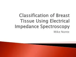
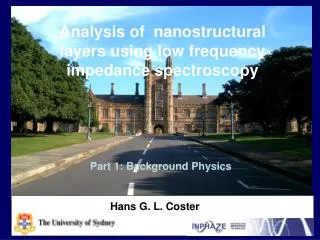
Analysis of nanostructural layers using low frequency impedance spectroscopy. Part 3: Phenomenological Impedances. Hans G. L. Coster. Phenomenological Impedances. Phenomenological impedances are not necessarily related to dielectric substructure. Manifest when:.

E N D
Analysis of nanostructural layers using low frequency impedance spectroscopy Part 3: Phenomenological Impedances Hans G. L. Coster
Phenomenological Impedances Phenomenological impedances are not necessarily related to dielectric substructure. Manifest when: (1) The properties of the material is modulated by the electric current passing through the material and (2) The changes in the properties are time dependent Phenomenological impedances are strongly frequency dependent (decrease with increasing frequency) and are generally seen at low frequencies Can provide useful information about charge carrier transport processes
Phenomenological impedance of a light bulb If the filament of the light bulb was a simple resistor then the current would be given by: However, the filament heats up because of the energy dissipation of the electric current and the resistance increases with temperature At low frequencies the temperature goes up and down during each cycle. The resistance changes with time during each cycle. Heating is rapid because the specific heat of the filament is small. Cooling is slower because the heat must be radiated away. At high frequencies (> ~10Hz) there is insufficient time for the filament to cool and it attains a constant, high, temperature.
V= 240 V AC Electrical properties of a light bulb Consider a 60 Watt light bulb under normal (50Hz) operating conditions When cold the resistance is ~ 100 W Maximum heating here Distorted sinewave With phase lead At low frequencies it appears as an inductor
Photo-voltaic Cells: Basic structure n p Y Electric potential profile Depletion Layer
Dielectric Structure: Equivalent circuit layers n p Depletion Layer
Conductance dispersion with frequency 2 layer model fitted to data
Capacitance Dispersion with frequency 2 layer model fitted to data We will initially look at the frquencies > 1 Hz
Basic Parameters for Cell determined by the INPHAZE dielectric structure refinement software Depletion Layer Capacitance : 3.10 x 10⁻³ Fm-2 343 nm Conductance: 13.3 S m-2 p type Si material Capacitance : 0.13 x 10⁻³ Fm-2 842 nm Conductance: 630 Sm-2
Diffusion and Recombination Complex Elements Current C* electrode Back diffusion G* recombination
Narrower depletion layer Photo-voltaic Cells n p Y Potential with forward bias Depletion Layer It takes time for holes and electrons to diffuse into the depletion region. The properties are therefore both time dependent and current dependent giving rise to a phenomenological impedance with a phase lag that will manifest at very low frequencies
Transport / Diffusion Capacitance and Conductance Data shows very large (3 orders of magnitude) dispersion of capacitance at frequencies < 1 Hz. Addition of an element with complex capacitances and conductances to model the charge injection transport polarisation allows that process to be characterized.
Equivalent circuit n p electrode C* G* C*=CR + j CX Depletion Layer G* = GR+ jGX
Cell Data Derived Depletion Layer Capacitance : 3.10 x 10⁻³ Fm-2 343 nm Conductance : 13.3 S m-2 (conductivity 4.7 x 10- 6Sm-1) p type Si material Capacitance : 0.13 x 10⁻³ Fm-2 842 nm Conductance : 630 Sm-2 (conductivity 43 x 10- 3 Sm-1) Transport number/Diffusion : Impedance element C*=-0.0140 - j. 0.0310 Fm-2 G*= 150x104 + j.7.30x 108 Sm-2
Conductance vs DC bias p type semiconductor layer (film) Depletion layer
The Spectrometer Impedance range: 0.1 -1010W Frequency: < 10-2 – 106 Hz Impedance precision: 0.002% Phase resolution: 0.001 o Inphaze.com.au