Download
1 / 22
220 likes | 311 Views
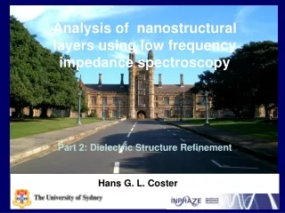
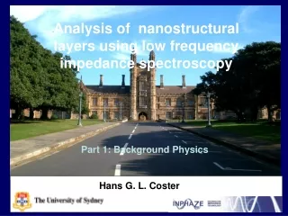
Analysis of nanostructural layers using low frequency impedance spectroscopy. Part 1: Background Physics. Hans G. L. Coster. Sinewave signal generator. voltage. Response of materials to AC currents. Current. Phase shift. Shift in relative magnitude. Electrical Circuit Equivalents.

E N D
Analysis of nanostructural layers using low frequency impedance spectroscopy Part 1: Background Physics Hans G. L. Coster
Sinewave signal generator voltage Response of materials to AC currents Current Phase shift Shift in relative magnitude
Impedance of capacitance elements C = Q/V Sinusoidal currents Same form as:
But we have that Hence Impedance of a capacitance element (Ohms’s Law)
current Impedance of capacitance elements C = Q/V The voltage lags behind (phase lags) the current
i1 R1 RT i2 R2 i V i V Parallel Circuits
ZC ZR ZT Parallel impedances
C ZC 1 ZR G 1 ZT Circuit elements to represent Layers Real Part Imaginary Part
Real part q ZT Imaginary part Real part q jwC YT G Imaginary part Phase relationships We measure ZT and q But it is simpler to work in terms of Admittances (Y= 1/Z) For a single “layer” containing parallel R and C elements :
C 1 G 1 C1= 0.006 F/m2 G1 = 0.003 S/m2 C2=0.059 F/m2 G2=4.35S/m2 Detecting substructure with Impedance Spectroscopy Homogeneous film Film with two homogeneous sub-structural layers Consider an example with the following dielectric parameters:
Impedance Spectroscopy: Dispersion of Impedance with frequency 100 10 1 0.1 G 1 Impedance G G 1 2 C 1 C C 2 1 0.1 1 10 100 1000 Frequency - Hz Conclusion: The impedance as a function of frequency does not allow us to discriminate between the single and 2 layer structures.
Impedance Spectroscopy: Capacitance dispersion with frequency G 1 G G 1 2 C 1 C C 2 1 0.0060 0.0059 0.0058 0.0057 0.0056 0.0055 Capacitance – mF m-2 0.1 1 10 100 1000 Frequency - Hz The capacitance as a function of frequency allows the single and 2 layered structure to be readily distinguished.
Impedance Spectroscopy: Conductance dispersion with frequency G 1 G G 1 2 C 1 C C 2 1 0.040 0.035 0.030 0.025 0.020 0.015 0.010 0.005 Conductance – S m-2 0.1 1 10 100 1000 Frequency - Hz The conductance as a function of frequency also allows the single and 2 layered structure to be readily distinguished.
A two layer sandwich Whilst C1, G1, C2, G2 are frequency independent, C and G for the combination is frequency dependent
SiO2 Silicon Wafer Silicon Wafer UV SiH SiH 40% NH4F Silicon Wafer Alkane layers on silicon
Organic films on Silicon substartes C monolayer G solution G monolayer Decane layer attached to Si The Born energy for ion partitioning into the alkane layer is very high. Therefore the electrical conductance of this layer will be very low. More info on Born Energy Silicon [111]
The Spectrometer Impedance range: 0.1 -1010W Frequency: < 10-2 – 106 Hz Impedance precision: 0.002% Phase resolution: 0.001 o Inphaze.com.au
Ion Partitioning into an organic film + + External solution Organic film Ion in water Image of ion in dielectric em ~ 2 -3 for hydrophobic films ew=80
Ion partitioning into molecular films The Born Energy arising from image forces on the ions is: For a K+ ion in a alkane layer, WB ~ 3 eV Recall that kT~ 0.025 eV at room temperature So that the partitioning goes as ~ e-120 !! Return to Main It will be a very poor electrical conductor!