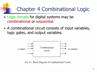
Module Design for Decoders and Adders in Combinational Logic Circuits
Learn to design more complex decoders, realize functions, use multiplexers, and implement adders efficiently with propagation delays and gate configurations. Explore ripple-carry, pseudo-parallel, and fully parallel adders, as well as look-ahead adder concepts. Discover binary subtraction and two's complement arithmetic overflow detection in integrated circuits. Enhance your understanding of combinational logic with practical examples.

Module Design for Decoders and Adders in Combinational Logic Circuits
E N D
Presentation Transcript
Use a 74151A multiplexer to Realizef(x1,x2,x3) = m(0,2,3,5) Figure 4.30
Half Adders Figure 4.35 (a) -- (c)
Full Adders Figure 4.35 (d) -- (g)
Ripple Carry Adder Figure 4.36
Addition Time for a Basic Ripple-Carry Adder Let tgate = the propogation delay through a typical logic gate Half adder propagation delays tadd = 3 tgate tcarry = 2 tgate Full adder propagation delays tadd = 3 tgate tcarry = 2 tgate Ripple-Carry Adder (n-bits) tadd = (n - 1)2 tgate + 3 tgate = (2n + 1) tgate
SN7482 Two-Bit Pseudo Parallel Adder Module Package Pin Configuration
SN7482 Two-Bit Adder -- Logic Equations C1 = C0A1 + C0B1 + A1B1 (4.20) 1 = C0C1 + A1C1 + B1C1 + A1B1C0 = C1(C0 + A1 + B1) + A1B1C0 = (C0+A1)(C0+B1)(A1+B1) (C0 +A1+B1) +A1B1C0 = (C0+ A1B1)(A1+B1)(C0 +A1+B1) +A1B1C0 (4.21) = [C0(A1+B1)+ C0A1B1](A1+B1)+A1B1C0 = C0A1B1+C0A1B1+C0A1B1+A1B1C0 = C0 A1 B1 Similarly C2 = C1A2 + C1B2 + A2B2 (4.22) 2 = C1 A2 B2
Add Time for SN7482 Adder Circuits SN7482 propagation delays t1 = 5 tgate tC1 = 2 tgate t2 = 6 tgate tC2 = 4 tgate SN7482-based ripple-carry adder (n-bits) tadd = (2n + 2)tgate
SN7483 Four-Bit Adder Module Package Pin Configuration
SN7483 Four-Bit Adder -- Logic Equations Pi = (BiAi)(Ai + Bi) = (Ai + Bi)(Ai + Bi) = Ai Bi (4.24) i = Pi Ci-1 = Ai Bi Ci-1 (4.25) C1 = [C0(A1B1) + (A1 + B1)] = [C0(A1B1)](A1 + B1) = (C0+(A1B1))(A1 + B1) = C0A1 + C0B1 + A1B1 (4.26) Similarly Ci = Ci-1Ai + Ci-1Bi + AiBi
Add Times for SN7483 Adder Circuits SN7483 propagation delays t1 = 3 tgate t2 = t3 = t4 = 4 tgate tC1 = tC2 = tC3 = tC4 = 3 tgate SN7483-based Ripple-Carry Adder (n-bits) tadd = (3m + 1)tgate where m = n/4.
Fully Parallel Three-Bit Adder c0 = x0y0(4.30) s0 = x0 y0 c1 = x1y1c0’+x1y1c0+x1y1’c0+x1’y1c0 = x1y1+(x1y1)c0 = x1y1+(x1y1)(x0y0) (4.31) s1 = x1y1c0 = x1y1 x0y0 c2 = x2y2+(x2y2)c1 = x2y2+(x2y2)[x1y1+(x1y1)(x0y0)] = x2y2+(x2y2)(x1y1)+(x2y2)(x1y1)(x0y0) (4.32) s2 = x2y2c1 = x2y2[x1y1+(x1y1)(x0y0)]
Add Time for a Fully Parallel Adder Assuming a three-level realization tadd = 3tgate However, the fan in requirements become impractical as n increases.
Carry Look-Ahead Adders -- Basic Idea Recall that ci = xiyi + xici-1 + yici-1 = xiyi + xiyici-1 + xiyici-1 + xiyici-1 + xi yici-1 = xiyi + xiyici-1 + xi yici-1 = xiyi + (xiyi + xi yi)ci-1 = xiyi + (xiyi)ci-1 Let gi = xiyi [carry generate] (4.33) pi = xiyi [carry propagate] (4.34) Then ci = gi + pi ci-1 si = pi ci-1 (4.38)
Carry Look-Ahead Adders -- Three-Bit Example c0 = g0 (4.35) s0 = p0 c1 = g1 + p1c0 = g1 + p1g0 (4.36) s1 = p1 c0 c2 = g2 + p2c1 = g2 + p2(g1 + p1g0) = g2 + p2g1 + p2p1g0 (4.37) s2 = p2 c1
Carry Look-Ahead Adder Design (c) Figure 4.39
Add Times for Carry Look-Ahead Adders Adder modules tg = tp = ts = tgate CLA module tc = 2 tgate Overall tadd = tgate + 2 tgate + tgate = 4 tgate
Binary Subtraction Circuits Recall that (R)2 = (P)2 - (Q)2 = (P)2 + (-Q)2 = (P)2 + [Q]2 = (P)2 + (Q)2 + 1 For an SN7483 adder ()2 = (A)2 + (B)2 + (C0)2 (4.39) where = 4321, A = A4A3A2A1, and B = B4B3B2B1 If C0 = 0, A = P, and B = Q, then ()2 = (P)2 + (Q)2 . If C0 = 1, A = P, and B = Q, then ()2 = (P)2 - (Q)2 .
Two’s Complement Adder/Subtracter Figure 4.41
Arithmetic Overflow Detection an-1bn-1cn-2cn-1sn-1V 0 0 0 0 0 0 0 0 1 0 1 1 0 1 0 0 1 0 0 1 1 1 0 0 1 0 0 0 1 0 1 0 1 1 0 0 1 1 0 1 0 1 1 1 1 1 1 0
Overflow Detection Circuits Figure 4.42