Download
1 / 15
170 likes | 441 Views
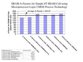
Memory design of 8 Mb using Loadless CMOS Four-Transistor SRAM Cell in a 0.25-um Logic Technology. Presented By: Gaurav Raja (2003EEN0013) Sonal Singh (2003EEN0007) Poornima Agarwal (2003EEN0029) GROUP – ‘E’. Specifications. No load SRAM Memory size = 8 Mb Word size = 2 bits

E N D
Memory design of 8 Mb using Loadless CMOS Four-Transistor SRAM Cell in a 0.25-um Logic Technology Presented By: Gaurav Raja (2003EEN0013) Sonal Singh (2003EEN0007) Poornima Agarwal (2003EEN0029) GROUP – ‘E’
Specifications • No load SRAM • Memory size = 8 Mb • Word size = 2 bits • No. of Blocks = 128 • Row Decoder = 8 x 256 • Column Decoder = 7 x 128 • Supply voltage = 1.8 V • Circuit works at 0.18 u tech, but we have designed for 0.25 u tech.
Design components • Access and precharge transistors are PMOS. • Row(word line) and column selector(bit line) are active low. • Regenerative amplifier (back to back inverter) works as sense amplifier. • 8 x 256 decoder is made using 2 x 4 decoder (pseudo Nor & Nand gates).
Simulation outputs for 1-bit(obtained from schematic) for Cbit=600fF
Measurement Results • Precharge time = 30 ns • Total write access time = 50ns • Total read access time = 50ns => 20 MHz • One cell area = 4.8 um x 3.25 um • Bit line capacitance of 1-bit = 0.1 fF
References • [1] K. Noda, K. Matsui, K. Imai, K. Inoue, K. Tokashiki, H. Kawamoto, • K. Yoshida, K. Takeda, N. Nakamura, T. Kimura, H. Toyoshima, Y. • Koishikawa, S. Maruyama, T. Saitoh, and T. Tanigawa, “A 1.9-m • loadless CMOS four-transistor SRAM cell in a 0.18-m logic technology,” • in IEDM Dig. Tech. Papers, 1998, pp. 74–75. • [2] H. Shimizu, K. Ijitsu, H. Akiyoshi, K. Aoyama, H. Takatsuka, K. • Watanabe, R. Nanjo, and Y. Takao, “A 1.4-ns access 700-MHz 288-kb • SRAM macro with expandable architecture,” in ISSCC Dig. Tech. • Papers, Feb. 1999, pp. 190–191. • [3] H. Hidaka, F. Fujishima, Y. Matsuda, M. Asakura, and T. Yoshihara, • “Twisted bitline architechture for multi-megabit DRAMs,” IEEE J. • Solid-State Circuits, vol. 24, pp. 21–28, Feb. 1989. • [4] K. Nakamura, K. Takeda, H. Toyoshima, K. Noda, H. Ohkubo, T. • Uchida, T. Shimizu, T. Itani, K. Tokashiki, and K. Kishimoto, “A • 500-MHz 4-Mb CMOS pipeline-burst cache SRAM with point-to-point • noise reduction coding I/O,” IEEE J. Solid-State Circuits, vol. 32, pp. • 1758–1765, Nov. 1997.