Pass Transistor Logic Cell Library
Pass Transistor Logic Cell Library. Group Members: Keith Benson Kofi Inkabi Ashley Nozine. Project Summary. Design basic cells that can incorporated into Cadence cell library. Incorporate cells into Cadence’s cell library. Compare technology mapped layout versus CMOS only Layout Power

Pass Transistor Logic Cell Library
E N D
Presentation Transcript
Pass Transistor LogicCell Library Group Members: Keith Benson Kofi Inkabi Ashley Nozine
Project Summary • Design basic cells that can incorporated into Cadence cell library. • Incorporate cells into Cadence’s cell library. • Compare technology mapped layout versus CMOS only Layout • Power • Area • Delay
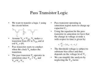
Cell Characteristics • 0.25um technology • Area • Height * Width • Height is constant at 54 = 6.75um • Delay • 50% Input 50% Output • Dynamic Power dissipation • PDyn = VDD * Iave • Iave = (IHL + ILH) / 2
Original Schedule • A: Project Proposal • B: Learn Cadence/Know Cadence Library Specs. • C: Build Cell layouts • D: Measure Cells for Power, Area, and Power • E: Receive Netlist and automatically generate layout of Technology Mapped cells • F: Compare Layout of PTL and CMOS cells against CMOS only cells
Revised Schedule • A: Locate tool to automatically generate layout from Netlist • B: Receive Netlist and automatically generate layout of Technology Mapped cells • C: Characterize Technology Mapped layout from netlist • D: Characterize CMOS layout from netlist • E: Compare Technology Mapped layout vs. CMOS only layout • F: Final Report