Download
1 / 18
310 likes | 827 Views
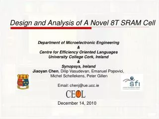
Design and Analysis of A Novel 8T SRAM Cell. Department of Microelectronic Engineering & Centre for Efficiency Oriented Languages University College Cork, Ireland & Synopsys, Ireland Jiaoyan Chen , Dilip Vasudevan, Emanuel Popovici, Michel Schellekens, Peter Gillen Email: chenj@ue.ucc.ie.

E N D
Design and Analysis of A Novel 8T SRAM Cell Department of Microelectronic Engineering & Centre for Efficiency Oriented Languages University College Cork, Ireland & Synopsys, Ireland Jiaoyan Chen, Dilip Vasudevan, Emanuel Popovici, Michel Schellekens, Peter Gillen Email: chenj@ue.ucc.ie December 14, 2010
Contents Motivation Architectures of 6T SRAM, 9T SRAM and our 8T SRAM Adiabatic and Non-Adiabatic Operations SNM Comparison Dynamic Power Static Power Conclusion
Motivation SOC Consumer Stationary Power Consumption (2008) Roadmap –Cell Area Trend(ITRS 2008) SRAM consumes a lot of power and area in chips. Our aim is to built an efficient SRAM. Consumer Portable Power Consumption Trend (ITRS 2008 update)
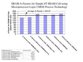
Conventional 6T SRAM Technology: 90nm,65nm,45nm, 28nm… Stability: Static Noise Margin (SNM) is getting Down. Leakage Power: a) Subthreshold leakage current b) Gate oxide leakage current 4
9T SRAM Features: a) 2 sub-circuits: Upper : Writing Lower: Reading b) Minimal Sizing for the upper part c) SNM is much better d) Lower leakage Power (in super cut-off mode) Z. Liu and V. Kursun, “Characterization of a novel nine-transistor sram cell,” IEEE Trans. Very Large Scale Integr. Syst., vol. 16, no. 4, pp. 488–492, 2008 5
Proposed 8T SRAM Features: a) 2 sub-circuits: Upper :1. No GND Connection 2. Add One Sharing transistor Lower: Using PMOS b) Half swing BL and BL’ return to VDD/2 after writing or reading. 6
Adiabatic Operations: Writing PMOS P3 is used to meet the Adiabatic Principle: No voltage difference before the transistor turns on
SNM Comparison (45nm) Proposed 8T SRAM Conventional 6T SRAM
Dynamic Power Comparison (1) 8*8 Array 1 Bit Cell
Dynamic Power Comparison (2) 67% 62%
Conclusion • Summary • Efficient 8T SRAM architecture • Improved SNM compared with 6T SRAM • Very Low Dynamic and Leakage power • Future work • Use 36nm, 28nm…Check performance particularly for leakeage • Further Enhance the Stability • Fabricate and validate the proposed architecture
Thank You Questions?