IC design options
160 likes | 344 Views
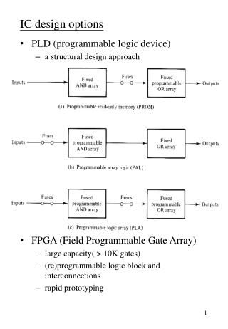
IC design options. PLD (programmable logic device) a structural design approach FPGA (Field Programmable Gate Array) large capacity( > 10K gates) (re)programmable logic block and interconnections rapid prototyping. VLSI design options Gate array

IC design options
E N D
Presentation Transcript
IC design options • PLD (programmable logic device) • a structural design approach • FPGA (Field Programmable Gate Array) • large capacity( > 10K gates) • (re)programmable logic block and interconnections • rapid prototyping
VLSI design options • Gate array • pre-fabed chip core contains a continuous array of transistors • only 2-5 masks are needed for (1) gate personalization and (2) interconnection • Standard cell • use a cell library which usually consists of SSI logic, MSI logic, and memory components • each gate type may provide variations of high-, normal- and low-power cells • Full-custom design • high-speed circuits • compact size • low productivity • A typical design procedure • Behavioral design (Verilog HDL) • Structural design (gate-level design) • Physical design • floor plan • place and route
5-7 Read-Only Memory (ROM) • ROM • a memory device of permanent binary information • n input lines: address • m output lines: word (data) • 2n distinct address = 2n distinct words • Another viewpoint • a decoder that generates the 2n minterms • plus m OR gates • can be used to implement any Boolean functions of n input variables • a fixed AND array and a programmable OR array n inputs m outputs 2n xm ROM
A 32x4 ROM • applications • permanent storage of program/data • display character fonts • a table-look-up log functions? • combination logic implementations • code conversion
combination logic implementation • store the truth table in a ROM
Examples 5-3 • generate the square of a 3-bit number
Types of ROMs • mask programming ROM • IC manufacturers • is economical only if large quantities • PROM: Programmable ROM • fuses • universal programmer • EPROM: erasable PROM • floating gate • ultraviolet light erasable • EEPROM: electrically erasable PROM • longer time is needed to write • flash ROM • limited times of write operations
2764 EPROM 8K x 8
Programmable Logic Array (PLA) • A ROM can implement any Boolean functions, but • an over-kill • logic functions can be minimized • don't-care conditions • converts a 12-bit card code to a 6-bit internal alphanumeric code (47 codes) • only 47 words of a 4096x6 ROM are used • PLA • only the needed product terms are generated • both the AND array and the OR array are programmable • n inputs, k product terms and m outputs • the number of fuses: 2n*k+k*m+m • area(cost) = (n+m)*k • a regular structure design
An example PLA • Types of PLA • mask-programmable • field-programmable logic array • A typical commercial PLA • more than 10 inputs • about 50 product terms
Programmable Array Logic • PAL • a programmable AND array and a fixed OR array • hundreds of gates interconnected through hundreds of electronic fuses • can replace 3-10 TTL IC's • is not as flexible as the PLA
can generate any product term • each OR has only three inputs • Commercial PAL • more than 8 inputs • some of the output terminals are sometimes bidirectional • each OR gate may have 8 inputs • the fuse pattern may be unreadable • output terminals may be latched • An example • w = S(2,12,13) x = S(7,8,9,10,11,12,13,14,15) y = S(0,2,3,4,5,6,7,8,10,11,15) z = S(1,2,8,12,13) • w = ABC'+A'B'CD' x = A+BCD y = A'B+CD+B'D' z = ABC'+A'B'CD'+AC'D'+A'B'C'D = w + AC'D'+A'B'C'D • using the output from w, the function z is reduced to three terms • if an input of the AND gates is not used, leave all the input fuses input intact