Computer Organization: CPU, Registers, and Control Unit
Explore the structure and function of computer components like the CPU, registers, ALU, and control unit. Learn how they work together in processing instructions and data efficiently. Understand clock cycles, system bus, and performance factors.

Computer Organization: CPU, Registers, and Control Unit
E N D
Presentation Transcript
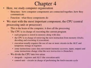
Chapter 4 • Here, we study computer organization • Structure: how computer components are connected together, how they communicate • Function: what these components do • We start with the most important component, the CPU (central processing unit or processor) • This is the brain of the computer, it does all the processing • The CPU is in charge of executing the current program • each program is stored in memory along with data • the CPU is in charge of retrieving the next instruction from memory (fetch), decoding and executing it (execution) • execution usually requires the use of one or more circuits in the ALU and temporary storage in registers • some instructions cause data movement (memory accesses, input, output) and some instructions change what the next instruction is (branches) • We divide the CPU into two areas • datapath – registers and ALU (the execution unit) • control unit – circuits in charge of performing the fetch-execute cycle
User registers These store data and addresses (pointers to data) These are manipulated by your program instructions Example: Add R1, R2, R3 R1 R2 + R3 Computers will have between 1 and hundreds of registers Possibly divided into data and address registers Registers are usually the size of the computer’s word size 32 or 64 bits today, previously it had been 8 or 16 bits Some machines use special-purpose registers each register has an implied usage Others have general-purpose registers use them any way you want to Control registers Registers that store information used by the control unit to perform the fetch-execute cycle PC – program counter – the memory location of the next instruction IR – instruction register – the current instruction being executed Status flags – information about the results of the last instruction executed (was there an overflow, was the result positive, zero or negative? Etc) Stack Pointer – location in memory of the top of the run-time stack (used for procedure calls and returns) Two Kinds of Registers
The ALU consists of circuits to perform arithmetic and logic operations Adder Multiplier Shifter Comparitor Etc… Operations in the ALU set status flags (carry, overflow, positive, zero, negative, etc) Also, possibly, temporary registers before moving results back to register or memory The control unit is in charge of managing the fetch-execute cycle It sends out control signals to all other devices A control signal indicates that the device should activate or perform it’s function For instance: Instruction fetching requires sending the PC value to main memory signaling memory to read when the datum comes back from memory, move it to the IR increment the PC to point to the next instruction These operations are controlled by the control unit Now the control unit decodes the instruction signals the proper ALU circuit(s) to execute it ALU and Control Unit
In order to regulate when the control unit issues its control signals, computers use a system clock At each clock pulse, the control unit goes on to the next task Register values are loaded or stored at the beginning of a clock pulse ALU circuits activate at the beginning of a clock pulse Typical clock speeds are based on the amount of time it takes to perform one of these actions (register or ALU) Clock performance is based on the number of pulses per second, or its Megahertz (or Gigahertz) rating This is a misleading spec The number of clock pulses (cycles) that it takes to execute one instruction differs from one computer to the next Assume computer A takes 10 clock cycles per instruction but has a 1 Gigahertz clock speed Assume computer B can execute 10 instructions in 11 cycles using a pipeline, but has a 250 Megahertz clock speed Which one is faster? B even though its clock is slower! The System Clock
Comparing Clocks • It is difficult to compute CPU performance just by comparing clock speed • You must also consider how many clock cycles it takes to execute 1 instruction • How fast memory is • How fast the bus is • Etc • The book offers an example comparing 286 multiply to a pentium multiply • In addition, there are different clocks in the computer, the Control Unit and the whole CPU are governed by the system clock • There is usually a bus clock as well to regulate the usage of the slower buses
System Bus connects the CPU to memory and I/O devices A bus is a collection of wires that carries electrical current The current is the information being passed between components typically the information is a datum or program instruction, but can also include control signals and memory or I/O addresses There are 3 parts to a bus the data bus (for both data and program instructions) the control bus (control signals from the Control Unit to devices, and feedback lines for acknowledging that the devices are ready or for interrupting the CPU) address bus (the address of the memory location or I/O device that is to perform the given data movement operation) Additionally, computers may have multiple buses local bus – connects registers, ALU and control unit together (also an on-chip cache if there is one) system bus – connects CPU to main memory expansion or I/O bus – connects system bus to I/O devices The Bus
Here we see the system bus in more detail The CPU connects to the bus through pins The bus is on the motherboard inside the system unit Main memory (a collection of chips) connects to this bus through pins The I/O subsystem connects to this bus through the expansion bus The bus carries three types of information the address from the CPU of the intended item to be accessed the control information (read versus write, or status information like “are you available?”) the data, either being sent to the device, or from the device to CPU The System Bus
More on Buses Point-to-point Buses • Buses connect two types of devices • Masters – those devices that can initiate requests (CPU, some I/O devices) • Slaves – those devices that only respond to requests from masters (memory, some I/O devices) • Some buses are dedicated • The bus directly connects two devices (point-to-point bus) • Most buses connect multiple components • Common pathway or multipoint Multipoint network Multipoint Expansion bus
Bus Interactions • Except for point-to-point buses, we have to worry about who gets to use the bus • Especially the expansion bus where multiple I/O devices may want to communicate between themselves and the CPU or memory at the same time – we need a form of bus arbitration • Daisy chain arbitration • each device has a bus request line on the control bus, when a device wants to use the bus, it places its request and the highest priority device is selected (this is an unfair approach) • Centralized parallel arbitration • the bus itself contains an arbiter (a processor) that decides – the arbiter might become a bottleneck, and this is also slightly more expensive • Distributed arbitration • the devices “vote” to determine who gets to use the bus, usually based on a priority scheme, again possibly unfair • Distributed arbitration using collision detection • it’s a free-for-all, but if a device detects that another device is using the bus, this device waits a short amount of time before trying again
I/O Subsystem • There are many different types of I/O devices, collectively known as the I/O Subsystem • Since I/O devices can vary greatly in their speed and usage, the CPU does not directly control these devices • Instead, I/O modules, or interfaces, take the CPU commands and pass them on to their I/O devices • One interface is in charge of one or more similar types of devices • To communicate to the right I/O device, the CPU addresses the device through one of two forms • Memory-mapped I/O • the interface has its own memory which are addressed as if they were part of main memory, so that some memory locations are not used, they are instead registers in the I/O interfaces • Isolated I/O • the CPU differentiates memory addresses from I/O addresses by having additional control lines indicating whether an address is meant for memory or I/O • we will explore I/O in more detail in chapter 7
I/O Devices and Bus • The expansion bus typically is the collection of expansion slots and what gets plugged into them • Here we see interface cards (or expansion cards), each with the logic to interface between the CPU and the I/O device (e.g., printer, MODEM, disk drive) • Some devices are placed on the card (MODEM), others are plugged into the card through ports
Memory Organization • Memory is organized into byte or word-sized blocks • Each block has a unique address • This can be envisioned as an array of cells, see the figure below • The CPU accesses memory by sending an address of the intended access and a control command to read or write • The memory module then responds to the request appropriately • A decoder is used to decode the binary address into a specific memory location
Dividing Memory Across Chips • Each memory chip can store a certain amount of information • However, architects decide how memory is spread across these chips • For instance, do we want to have an entire byte on a single chip, or spread a byte across 2 or more chips? • The figure to the right shows that each chip stores 2 Kbytes and with 16 rows and 2 columns of chips, we can store 64 Kbytes • Here, a word (16 bits) is stored in two chips in the same row
Interleaving Memory • Using high-order interleave, the address is broken into the chip followed by the location on the chip, giving a layout as shown above • The advantage of high-order interleave is that two different devices, working on two different areas of memory, can perform their memory accesses simultaneously • e.g., one device accesses address 5 and another accesses 31 • In low-order interleave, the address is broken up by location on the chip first, and the chip number last • Consecutive memory locations are on consecutive chips • The advantage of lower-order interleave is that several consecutive memory accesses can be performed simultaneously • For instance, fetching 4 consecutive instructions at one time
Interrupts • The last part of our computer organization is an interrupting mechanism • Left to itself, the CPU performs the fetch-execute cycle on your program repeatedly without pause, until the program terminates • What happens if an I/O device needs attention? • What happens if your program tries to do an illegal operation? • see the list on page 157 of types of illegal operations • What happens if you want to run 2 or more programs in a multitasking mode? • You cannot do this without interrupts • An interrupt is literally the interruption of the CPU so that it can switch its attention from your program to something else • an I/O device, the operating system, or another user program
The Interrupt Process • At the end of each fetch-execute cycle, the CPU checks to see if an interrupt has arisen • Devices send interrupts to the CPU over the control bus • If the instruction causes an interrupt, the Interrupt Flag (in the status flags) is set • If an interrupt has arisen, the interrupt is handled as follows • The CPU saves what it was doing (PC and other important registers are saved to the run-time stack in memory) • The CPU figures out who raised the interrupt and executes an interrupt handler to handle that type of interrupt • The interrupt handler is a set of code (part of the OS) stored in memory • While the interrupt is being handled, the CPU may choose to ignore or disable interrupts from interrupting the interrupt handler (known as a maskable interrupt) or may choose to handle a future interrupt (non-maskable interrupt) • Once the interrupt has been handled, the CPU restores the interrupted program by retrieving the values from the run-time stack
MARIE: A Simple Computer • We now put all of these elements together into a reduced computer • MARIE: Machine Architecture that is Really Intuitive and Easy • Unfortunately we will find that MARIE is too easy, it is not very realistic, so we will go beyond MARIE as well • We will explore MARIE’s • CPU (registers, ALU, structure) • Instruction set (the instructions, their format – how you specify the instruction, addressing modes used, data types available • Interrupts, I/O • Some simple programs in MARIE
Data stored in binary, two’s complement Stored programs 16-bit word size with word addressing (you can only get words from memory, not bytes) 4K of main memory using 12 bit addresses, 16-bit data 16-bit instructions (4 bits for the op code, 12 bits for the address of the datum in memory) Registers: AC (accumulator) – this is the only data register (16 bits) PC (12 bits) IR (16 bits) Status flags MAR (memory address register) – stores the address to be sent to memory, 12 bits MBR (memory buffer register) – stores the datum to be sent to memory or retrieved from memory, 16 bits 8-bit input and 8-bit output registers MARIE’s Architecture
MARIE CPU The structure of our CPU with the registers shown Notice that the MAR sends to memory, the MBR stores the datum being sent to memory or retrieved from memory, the InREG and OutREG receive data from and send data to I/O respectively The data pathways in the CPU from register to register or to the ALU or memory
MARIE’s Fetch-Execute Cycle PC stores the location in memory of the next Instruction 1) fetch instruction by sending the address to memory (PC to MAR to memory) 2) memory sends back instruction over data bus, to MBR, move it to IR, increment PC 3) Decode the instruction (look at op code, place 8-bit data address in MAR if needed 4) If operand required, fetch it from memory 5) Execute instruction 6) If necessary, process interrupt
Processing an Interrupt Which registers should we save? In MARIE, AC, PC (and SP if we have one) ISR is the interrupt service routine’s starting location, stored in a special place in memory called the vector table We explore this in detail in chapter 7
MARIE’s Instructions • move a datum from memory to AC or back (Load/Store) • perform + or – between AC and datum in memory • do I/O • skip over an instruction, jump to a different location in memory (used in if-else, loop instructions) • halt the program
Example: Add 2 Numbers This code will add the two numbers stored at memory location 104 and 105 Load 104 loads the AC with the value at 104 (0023) Add 105 adds to the AC the value at 105 (FFE9) Store 106 takes the value in the AC (000C) and moves it to location 106 Halt then stops the program
The Complete MARIE Instruction Set This figure shows the register movements (RTN – register transfer notation) required for each of the 15 instructions in MARIE’s instruction set
Loop Example We want to implement the following loop in MARIE code: for(i=0;i<n;i++) sum += i; assume that i is stored at 200, n at 201, sum at 202, that the variable one is stored at 203 storing the value 1, and that the code starts at address 100 (all addresses are hex addresses) 100: Clear 1010 000000000000 A000 101: Store i 0010 001000000000 2200 102: Clear 1010 000000000000 A000 103: Store sum 0010 001000000010 2202 104: Loop: Load i 0001 001000000000 1200 105: Subt n 0100 001000000001 4201 106: Skipcond 00 1000 000000000000 8000 107: Jump xout 1001 000100001110 910F 108: Load i 0001 001000000000 1200 109: Add sum 0011 001000000010 3202 10A: Store sum 0010 001000000010 2202 10B: Load i 0001 001000000000 1200 10C: Add one 0011 001000000011 3203 10D: Store i 0010 001000000000 2200 10E: Jump Loop 1001 000100000100 9104 10F: Xout: Halt
Two More Examples if (x = = y) x = x * 2; else y = y – x; Load x Subt y Skipcond 01 Jump Else Load x Add x Store x Jump End Else: Load y Subt x Store y End: Halt Code to perform z = x * y. This code wipes out the original value of y. Clear Store z Loop: Load y Skipcond 10 Jump Done Subt 1 Store y Load x Add z Store z Jump Loop Done: Halt Other examples located on the website
Assemblers and Assembly Language • Compare the machine code to the assembly code • You will find the assembly code much easier to decipher • Mnemonics instead of op codes • Variable names instead of memory locations • Labels (for branches) instead of memory locations • Assembly is an intermediate language between the instruction set (machine language) and the high-level language • The assembler is a program that takes an assembly language program and assembles it into machine language, much like the compiler compiles a high-level language program • Today we have very sophisticated compilers and provide highly optimized code, so there is no need to ever program in assembly language • We cover it here so that you can have a better understanding of how the CPU works
Fetch-Execute Cycle Revisited • Recall that the control unit causes the fetch-execute cycle to be performed • How is the fetch process carried out? • Once an instruction is fetched, it is decoded and executed, how? • To answer these questions, we must implement the control unit • Control units are implemented either in a hardwired form or by microprogramming • Hardwired – each operation including the execution of every machine instruction uses a decoder to translate the op code into control sequences (such as move PC to MAR, signal memory read, move MBR to IR, increment PC) • This decoder can be extremely complicated, as you might expect, as every instruction must be converted directly into control signals • Microprogrammed – a ROM is used to store microprograms, one for each machine instruction
Hardwired Control Unit The hardwired control unit is one big circuit Input is the instruction from the IR, status flags and the system clock and output are the control signals to the registers and other devices
Microprogrammed Control Unit The control store is a ROM that stores all of the microprograms One microprogram per fetch-execute stage, and one per instruction in the instruction set Receive an instruction in IR Start the microprogram, generating the address, fetching the instruction from the ROM and moving it to the microinstruction buffer to be decoded an executed This process is much more time consuming than the hardwired unit, but is easier to implement and more flexible
Portion of MARIE’s Control Store See table 4.8 (p. 221) which shows the RTN for each entry under MicroOp2
Complex (CISC) Microprogrammed control unit Large number of instructions (200-500) Instructions can do more than 1 thing (that is, an instruction could carry out 2 or more actions) Many addressing modes Instructions vary in length and format This was the typical form of architecture until the mid 1980s, RISC has become more popular since then although most architectures remain CISC Reduced (RISC) Hardwired control unit Instruction set limited (perhaps 80-100 instructions) Instructions rely mostly on registers, memory accessed only on loads and stores Few addressing modes Instruction lengths fixed (usually 32 bits long) Easy to pipeline for great speedup in performance CISC vs. RISC
Real Architectures • MARIE is much too primitive to be used but it shares many features with other architectures • Intel – started with the 8086 in 1979 as a CISC, has progressed over time in complexity and capability, 4 general purpose registers, originally 16 bit, expanded to 32 bit with 80386 and floating point operations in pentium, pentium II and later include many RISC features such as pipelining, superscalar and speculative execution • MIPS – RISC architecture, 32 bit early on, now 64 bit, 32 registers, advanced pipelining with superscalar and speculative execution