Operational Amplifier (2)
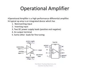
Operational Amplifier (2). Chapter 9. Topics. Two-Stage Op-Amps Gain-Boosting Input Rage Limitation Slew Rate Power Supply Rejection Noise. Simple Implementation of a Two-Stage Op-Amp. Stage 1. Two-Stage Op-Amp Employing Cascoding. (small voltage swings). High gain stage.

Operational Amplifier (2)
E N D
Presentation Transcript
Operational Amplifier (2) Chapter 9
Topics • Two-Stage Op-Amps • Gain-Boosting • Input Rage Limitation • Slew Rate • Power Supply Rejection • Noise
Two-Stage Op-Amp Employing Cascoding (small voltage swings) High gain stage
Gain-Boosting • Idea behind gain boosting: increase the output impedance without adding more cascode devices.
Increasing the Output Impedance by Feedback Io Io is sensed by ro1, convert into voltage, subtracted Vb. Current-Voltage Feedback. Loop gain Increased by A1
Implementation (Small signal gain) Vout, min=VOD2+VGS3
Differential Implementation Minimum voltage at the drain of M3:
Folded Cascode Gain Boosting (Minimum Vx)
Input Range Limitations (Vin is input limited, as opposed to output limited)
Extension of input CM Range As Vin, cm →VDD, the PMOS input pair turns off. As Vin, cm→0, the NMOS input pair turns off.
Slew Rate • “Linear settling” is only applicable to sufficiently small inputs. • With a large input step, the output displays a linear ramp with a constant slope. The slope of the ramp is called the slew rate. • While the small signal bandwidth of a circuit suggests a fast time-domain response, the large signal speed may be limited by the slew rate simply because the current available to charge the dominant capacitor is limited.
Response of a linear circuit to an input step • The slope of the step response is proportional to the final value of the output; if we apply a larger input step, the output rises more rapidly.
Slewing • Slewing is a nonlinear phenomenon. If the input doubles, the output level does not double at all points because the ramp exhibits a slope independent of the input!
Power Supply Rejection • Op-Amps are supplied from noisy lines, and must “reject” the noise adequately. • Power Supply Rejection Ratio (PSRR) is defined as the gain from input to the output divided by the gain from the supply to the output.
Example (1) If M3 and M4 carry the same amount current, then VGS3=VGS4=VDS3=VDS4. Therefore VX=Vout At low frequencies, M3 carries ISS/2, VGS3 is constant for a bias current of ISS/2, therefore, noise from VDD couples directly to VX. Since VX=Vout, the VDD noise is coupled to Vout, with a gain of unity. The PSRR at low frequencies:
Example (2) • Calculate the Low Frequency PSRR of the feedback circuit (KCL) (KVL)
Example (3) (Low frequencies analysis, C1 and C2 do not draw any current) (PSRR) β=C1/(C1+C2), Vout/Vin=1/β=1+C2/C1
Noise in a Telescopic Op-Amp (Do not contribute much noise)
Noise in a Telescopic Op-Amp Observation: 1. Low impedance path to output via M3. 2. DivdeVout, M1 by Av2 (Flicker noise) Account for M1 and M2
Rule of Thumb • Mentally change the gate voltage of each transistor by a small amount and predict the effect at the output.
Noise in a Folded Cascode Circuit Do not contribute much noise
Noise-Voltage Swing Trade-Off If the VOD of M9 and M10 is Reduced to increase output swing, the noise of M9 will increase.
Noise in a Two-Stage Op-Amp Noise of stage 2 not so significant
Summary (Telescopic) (Folded cascode, Only thermal noise is included) (Two Stage Op-Amp)