Chapter 2 Operational Amplifier Circuits
Chapter 2 Operational Amplifier Circuits. 2.1 Bias Circuit Suitable for IC Design. The bias circuits used to bias discrete BJT need large number of resistors as well as large coupling and bypass capacitors Biasing in integrated-circuit design is based on the use of constant-current sources

Chapter 2 Operational Amplifier Circuits
E N D
Presentation Transcript
2.1 Bias Circuit Suitable for IC Design • The bias circuits used to bias discrete BJT need large number of resistors as well as large coupling and bypass capacitors • Biasing in integrated-circuit design is based on the use of constant-current sources • On an IC chip with a number of amplifier stages a constant dc current is generated at one location and is then reproduced at various other locations of biasing the various amplifier stages
The Diode-connected Transistor • Shorting the base and collector of a BJT together result in a two-terminal device having an i-v characteristic identical to the iE-vBE characteristic of the BJT
The Current Mirror • The current mirror in its simplest form consists of two matched transistors Q1 and Q2 with their bases and emitters connected together (same VBE). • One of the transistors, Q1 is connected as diode by shorting its collector to its base.
Derivation • Since Q2 is identical to Q1, IE2 = IE1 = Iref. Therefore, Io is approximately equal to Iref(as long as Q2 is maintained in the active region.)[ic=Is eVBE/VT (1+VCE/VA)]
Effect of Finite • IREF = (2+) / (1+) IE and • I0 = / (1+) IE • ThereforeI0 / IREF = /(+2) = 1 / (1+2/) which approaches unity for >>1. • = 100 results in 2% error.
Practical Side • Another factor that makes I0 unequal to IREF is the linear dependence of the collector current of Q2, which is I0, on the collector voltage of Q2. • In fact, even if we ignore the effect of finite and assume that Q1 and Q2 are perfectly matched, the current I0 will be equal to IREF only when the voltage at the collector of Q2 is equal to the base voltage. • As the collector voltage is increased, I0 increases. The dependence of I0 on V0 is determined by r0 of Q2.
2.2 The Widlar Current Source • Simple current source • IREF, determined by a resistor R connected to the positive power supply VCC. The current IREF is given by • IREF = (VCC – VBE)/R • The circuit will operate as a constant-current source as long as Q2 remains in the active region-that is, for V0 VBE. The output resistance of this current source is r0 of Q2.
Current Steering Circuits • IREF = VCC + VEE - VEB1 - VBE2/R • IREF = I1. • I3 = 2IREF • Q3 sources its current to parts of the circuit whose voltage should not exceed VCC - VEB3. • Q4 sinks its current from parts of the circuit whose voltage should not decrease below–VEE + VBE4.
Improved Current Source Circuit • I0/IREF 1/(1+2/2) • which means that the error due to finite has been reduced from 2/ to 2/2, a tremendous improvement • An alternative mirror circuit that achieves both base-current compensation and increased output resistance is the Wilson mirror
The Widlar Current Source • VBE1 = VT ln (IREF/IS) • VBE2 = VT ln (I0/IS), • VBE1 - VBE2 = VT ln (IREF/I0) • From the circuit, • VBE1 = VBE2 + I0RE • and so, I0RE = VT ln (IREF/IO)
The Widlar Current Source • Widlar circuit allows generation of a small constant current using relatively small resistors which results in considerable savings in chip area. Another characteristic of a Widlar circuit is that its output resistance is high due to the presence of emitter resistance RE
Output Resistance Calculation • vx = -v - (gm + 1/RE')vr0 • And a node equation at C provides • ix = gmv - (gm + 1/RE')v • Hence the output resistance is • R0 = vx/ix = RE’ + (1 + gmRE’) r0 (1 + gmRE’) r0
Example • Fig 2.10 shows two circuits for generating a constant current I0 = 10 A. Determine the values of the required resistors assuming that VBE is 0.7 V at a current of 1 mA and neglecting the effect of finite .
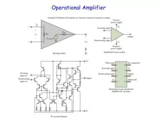
2.3 The Differential Amplifier • The output of a differential amplifier is proportional to the difference between the two input voltages
Rs = Rg + rb • v1 = ib1Rs + ie1re + ixRx • v2 = ib2Rs + ie2re + ixRx • ix = ie1 + ie2 • ie1 = (+1) ib1 • ie2 = (+1) ib2 • these give • v1 - v2 = (ib1-ib2)[Rs + (+1) re] • or, ib1 - ib2 = (v1-v2)/Rs + (+1) re • vo = ibRL- ib2RL • = RL (v1 - v2)/Rs + (+1) re • vo v1-v2
Small Signal Analysis • Assume two perfectly matched transistors Q1 and Q2 (have identical values of , re etc.) connected in differential amplifier configuration. Consider a small signal vi1 applied to input 1, and input 2 grounded. Assuming the constant current source to be ideal, it presents an infinite impedance (open circuit) to an ac signal [since the current has to be constant ac signal cannot flow through it], so its presence need not be considered.
Small Signal Analysis • Take re1 = re2, then vbe1 = -vbe2 = vi1/2 [(vi1/2re) re] • Vbe1 is in-phase with, and one half the magnitude of vi1. vbe2 is out of phase with vi1. The output voltage vo1 is amplified and inverted version of the input vi1 [common emitter amplifier action]. • There will also be an output voltage at the collector of Q2 (vo2) and it is out of phase with ve2 ( out of phase with vo1). However, the magnitude of vo2 is equal to that of vo1, because the transistors Q1 and Q2 are matched.
Graphical Illustration • By superposition principle, it follows that, if both vi1 and vi2 were present at the same time, the resulting outputs would be exactly twice the level • Note that the voltage at each collector will be exactly 0, if the inputs are driven by in phase voltages of equal magnitude. In such a case, the input differential voltage as well as the output differential voltage will also be 0
Derivation in terms of circuit parameters • With Q2 base grounded, the resulting circuit is shown in figure. Neglecting ro at the collector of Q1, vo1/vbe1 -RC/re • Therefore, the voltage gain, vo1/vi1=-Rc/2re • Hence, (vo1 - vo2)/(vi1 - vi2) = -RC/re and vo1/(vi1 - vi2) = -RC/2re
DC analysis • IE = IE1 = IE2 = I/2 • Vo1 = Vo2 = VCC - ICRC • With IC IE = I/2, • Vo1 = Vo2 = VCC - I/2 RC • RE = 0.026/IE = 0.026/(I/2)
2.4 Active Loads • Transistors occupy much less silicon area than resistors, so many BJT ICs use BJT loads in place of the resistive loads, RC. In such circuits, the BJT load transistor is usually connected as a constant current source and thus presents the amplifier transistor with a very high resistance load (the output resistance of the current source). Thus amplifiers that utilize active loads can achieve higher voltage gains than those with passive (resistive) loads
Circuit with Active Load • Fig 2.16 shows the active load differential amplifier circuit with transistors Q1 and Q2 forming the differential amplifier circuit with transistors Q1 and Q2 forming the differential pair biased with constant current I. The load circuit consists of transistors Q3 and Q4 connected in a current mirror configuration. The output is taken single-endedly from the collector of Q2
Consider the first case when no input signal is applied (that is the two input terminals are grounded). The current I splits equally between Q1 and Q2. Thus Q1 draws a current approximately equal to I/2 from the diode-connected transistor Q3. Assuming >>1, the mirror supplies an equal current I/2 through the collector of Q4. Since this current is equal to that through the collector of Q2, no output current flows through the output terminal. [In practical circuits, the dc quiescent voltage at the output terminal is determined by the subsequent amplifier stage]
Next consider a differential signal vd is applied at the input. Current signals gm(vd/2) will result in the collector of Q1 and Q2 with polarities indicated in figure. The current mirror reproduces the current signal gm(vd/2) through the collector of Q4. Thus at the output node we have two current signals that add together to produce a total current signal of gmvd. Now if the resistance presented by the subsequent amplifier stage is very large, the voltage signal at the output terminal will be determined by the total signal current and the total resistance between the output terminal and ground Ro; that is • vo = gmvd Ro • Ro = parallel equivalence of the output resistance of Q2 and the output resistance of Q4.
Since Q2 is operating in common emitter configuration, its output resistance will be equal to r02. Also, the output resistance of basic current mirror is equal to ro of Q4, that is ro4. • Ro = ro2||ro4 = ro/2 • and vo = gmvd(ro/2) • voltage gain vo/vd = gmro/2 • Substituting gm = IC/VT and ro = VA/IC,where IC = I/2, • gmro = VA/VT = constant for given transistor. • Typically VA =100v, leading to gmro = 4000 and a stage voltage gain of about 2000. • Without the current mirror (that is, using only a simple current source) the voltage gain would be half the value found above
Circuit Calculations • 2IE1 = (VEE-VBE)/RE1 • IE1 = 0.988 mA • IC1 = IC2 • VC1 = VC2 = VCC - IC1RC1 • = 7.83V • 100 * IE3 + 15k * 2IE3 = 17.12 • IE3 = 0.569 mA = IE4 • VC3 = VC4 = VCC - RC3IC3 = 9.32V • VCE1 = VCE2 = 8.545V • VCE3 = VCE4 = 2.2V
Findings • Because of direct coupling, the dc levels at the emitters rises from stage to stage. This increase in dc level tends to shift the operating point of the succeeding stages and, therefore, limits the output voltage swing and may even distort the output signal. • The voltage at the output terminal of the second stage is well above ground. This dc level is undesirable because it tends to limit the p-to-p output voltage swing without distortion and also contributes to the error in the dc output signal. • Therefore a final stage should be included to shift the output dc level at the second stage down to zero volts. Such a stage is referred to as a level translator of shifter.
Level Shifting Circuits • There are a variety of level shifting circuits. An emitter follower with a voltage divider is the simplest among them. The output of the second differential stage is input to Q5. Thus a positive 9.32V at the output terminal (VC4) of the second stage can produce zero volts at the junction of R1 and R2 with proper selection of components.
Better Level Shifting Circuits • RE = 0.7/3mA = 233.3 (use 270) • Taking I2 = IE6 • R2 = (VEE - 1.4)/IE6 =2.87k (use 2.7k) • Take VBE5 = 0.7V which gives • VE5 = 9.32 - 0.7 = 8.62V • IE5 = IC6 3mA; VC6 = 0V • R = 8.62/3mA = 2.87k(use 3k potentiometer)
Better Level Shifting Circuits • I2 = (VEE - 0.7)/R2 • R2 = 9.3/3mA = 3.1k • and R = 8.62/3mA = 2.87k • Better results are attained by using an emitter follower with a diode constant current bias or a current mirror instead of the voltage divider.
2.6 Output Stages • The purpose of the output stage is to provide the amplifier with a low output resistance. In addition, the output stage should be able to supply relatively large load currents without dissipating a large amount of power in the IC.
Circuit Analysis of an operational amplifier • Q1 and Q2 form the input differential stage. The signal inputs are grounded for the purpose of dc analysis and we wish to verify that the output is zero V under those conditions. The 50 resistor in the emitters of Q1 and Q2 serve to increase the amplifier’s input impedance and to make the stage less sensitive to variations inre. Q3 and Q4 form an unbalanced differential stage that provides additional voltage gain. Q5 performs the level-shifting function. Q6 is an emitter follower whose output is the output of the operational amplifier. Q7 and Q8 are constant-current sources that bias the two differential stages. These sources share a common voltage divider across the transistor bases.
DC analysis • The voltage divider across the base of Q7 sets the base voltage to • VB7 = [10k/(10k + 4.7k)](-15V) = -10.2 V • Therefore, the emitter voltage of Q7 isVB7 - 0.7 = -10.9 V, and the emitter current is • IE7 = (|VEE| - |VE7|)/RE7 = (15 - 10.9)V/10.2k = 0.4 mA
DC Analysis Contd. • Assuming matched conditions, this current divides equally between Q1 and Q2, and, sinceIC1 = IC2 IE2 = (0.4 mA)/2 = 0.2 mA, the collector voltages at Q1 and Q2 are VC1 = VC2 = VCC-ICRC = 15- (0.2 mA)(25k) = 10 V. Since the bases of Q1 and Q2 are grounded, their emitters are at approximately 0 - 0.7V = -0.7 V, and the small drop across each 50 resistor [(50) x (0.2 mA) = 0.01 V] sets the collector of Q7 at about the same voltage (-0.71 V).
DC Analysis Contd2. • We can now analyze the bias of the second differential stage. Since VB8 = VB7 = -10.2 V, the emitter of Q8 is at VE8 = VB8 –0.7 = -10.9V. Then • IE8 = (|VEE| - |VE8|)/RE8 = (15 - 10.9)/2.27 k = 1.8 mA • The 1.8 mA divides equally between Q3 and Q4, so the collector voltage of Q4 is VC4 = VCC - ICRC = 15 - (0.9 mA)(3.3k) = 12 V. Since the bases of Q3 and Q4 are directly-coupled to the collectors of Q1 and Q2, the base voltages are VB3 = VB4 =10 V. The emitter voltages are VE3 = VE4 = 10 - 0.7 = 9.3 V.
DC Analysis Contd3. • The base of the level-shifting PNP transistor, Q5, is direct-coupled to Q4, so VB5 = 12 V. Therefore, Q5 has emitter voltage VE5 = VB5 + 0.7 = 12.7 V. The emitter current in Q5 is • IE5 = (VCC - VE5)/RE5 = (15-12.7) / 1.53 = 1.5 mA • Since IC5 IE5, the collector of Q5 is at VC5 = (IC5)(10.47 k) - VEE = (1.5 mA)(10.47 k) –15 = +0.7 V. • Q5 accomplishes level shifting because its collector can go both positive and negative. • Since the base of the output transistor, Q6, is at 0.7 V, its emitter is at 0V, and we see that the amplifier output is 0V. The bias current in Q6 is (0 – VEE) / 5 = 15 / 5 = 3 mA.