Download
1 / 30
310 likes | 499 Views
Integration of cache and MIPS Pipeline. Data-path control unit design Pipeline stalls on cache misses. Actions Needed on an I-Cache Miss. 1. Compute the value of PC-4. 2. Instruct the main memory to perform a read and wait for the memory to complete its access.

E N D
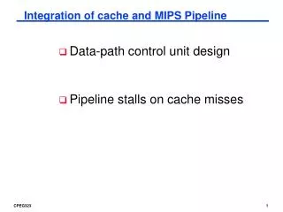
Integration of cache and MIPS Pipeline • Data-path control unit design • Pipeline stalls on cache misses
Actions Needed on an I-Cache Miss 1. Compute the value of PC-4. 2. Instruct the main memory to perform a read and wait for the memory to complete its access. 3. Write the cache entry, putting the data from memory in the data portion of the entry, writing the upper bits of the address (from the ALU) into the tag field, and turning the valid bit on. 4. Restart the instruction execution at the first step, which will re-fetch the instruction, this time finding it in the cache.
A Case Study: DEC Station 3100 • Separate I-Cache and D-Cache • “Write-through” policy • One-word-line simplifies write-miss handling
How to Handle Read/Write • Write Write-through: for both write hit/miss 1. Index the cache using bits 15-2 of the address. 2. Write both the tag portion (using bits 31 - 16 of the address) and the data portion with the word. 3. Also write the word to main memory using the entire address.
Performance Penalty due to Write-Through on DEC Station 3100 • CPI without cache misses: 1.2 (gcc), but with each write takes 10 cycles: CPI becomes 2.3 (gcc) Note: in gcc, 11% of instructions are stores, each takes 10 cycles • Solution: write buffers (in DEC Station 3100: size=4)
Large and Fast: Exploiting Memory Hierarchy Instruction and data miss rates for the DECStation 3100 when executing the different programs. The combined miss rate is the effective miss rate seen. It is obtained by weighting the instruction and data individual miss rates by the frequency of instruction and data references.
Combined I-Cache/D-Cache? • Hit ratio: Combined may be better: In DECStation 3100: 4.8% vs 5.4% • Bandwidth considerations
CPU CPU CPU Multiplexer Cache Cache Cache Bus Bus Bus Memory bank 0 Memory bank 1 Memory bank 2 Memory bank 3 Memory Memo- ry b. Wide memory organization c. Interleaved memory organization a. One-word-wide memory organization High-Bandwidth Design Alternatives The primary method of achieving higher memory bandwidth is to increase the physical or logical width of the memory system. In this figure there are two ways in which the memory bandwidth is improved. The simplest design, (a), uses a memory where all components are one word wide; (b) shows a wider memory, bus, and cache while (c) shows a narrow bus and cache with an interleaved memory.
Review: Major Components of a Computer Processor Devices Control Input Memory Datapath Output
µProc 55%/year (2X/1.5yr) DRAM 7%/year (2X/10yrs) Processor-Memory Performance Gap “Moore’s Law” Processor-Memory Performance Gap(grows 50%/year)
The “Memory Wall” • Logic vs DRAM speed gap continues to grow Clocks per DRAM access Clocks per instruction
Memory Performance Impact on Performance • Suppose a processor executes at • ideal CPI = 1.1 • 50% arith/logic, 30% ld/st, 20% control and that 10% of data memory operations miss with a 50 cycle miss penalty • CPI = ideal CPI + average stalls per instruction = 1.1(cycle) + ( 0.30 (datamemops/instr) x 0.10 (miss/datamemop) x 50 (cycle/miss) ) = 1.1 cycle + 1.5 cycle = 2.6 so 58% of the time the processor is stalled waiting for memory! • A 1% instruction miss rate would add an additional 0.5 to the CPI!
The Memory Hierarchy Goal • Fact: Large memories are slow and fast memories are small • How do we create a memory that gives the illusion of being large, cheap and fast (most of the time)? • With hierarchy • With parallelism
A Typical Memory Hierarchy • By taking advantage of the principle of locality • Can present the user with as much memory as is available in the cheapest technology • at the speed offered by the fastest technology On-Chip Components Control eDRAM Secondary Memory (Disk) Instr Cache Second Level Cache (SRAM) ITLB Main Memory (DRAM) Datapath Data Cache RegFile DTLB Speed (%cycles): ½’s 1’s 10’s 100’s 1,000’s Size (bytes): 100’s K’s 10K’s M’s G’s to T’s Cost: highest lowest
Inclusive– what is in L1$ is a subset of what is in L2$ is a subset of what is in MM that is a subset of is in SM 4-8 bytes (word) 8-32 bytes (block) 1 to 4 blocks 1,024+ bytes (disk sector = page) Characteristics of the Memory Hierarchy Processor Increasing distance from the processor in access time L1$ L2$ Main Memory Secondary Memory (Relative) size of the memory at each level
Memory Hierarchy Technologies • Caches use SRAM for speed and technology compatibility • Low density (6 transistor cells), high power, expensive, fast • Static: content will last “forever” (until power turned off) 21 Address Chip select 16 SRAM 2M x 16 Output enable Dout[15-0] Write enable Din[15-0] 16 • Main Memory uses DRAM for size (density) • High density (1 transistor cells), low power, cheap, slow • Dynamic: needs to be “refreshed” regularly (~ every 8 ms) • 1% to 2% of the active cycles of the DRAM • Addresses divided into 2 halves (row and column) • RASor Row Access Strobe triggering row decoder • CAS or Column Access Strobe triggering column selector
Memory Performance Metrics • Latency: Time to access one word • Access time: time between the request and when the data is available (or written) • Cycle time: time between requests • Usually cycle time > access time • Typical read access times for SRAMs in 2004 are 2 to 4 ns for the fastest parts to 8 to 20ns for the typical largest parts • Bandwidth: How much data from the memory can be supplied to the processor per unit time • width of the data channel * the rate at which it can be used • Size: DRAM to SRAM 4 to 8 • Cost/Cycle time: SRAM to DRAM 8 to 16
bit (data) lines Each intersection represents a 6-T SRAM cell or a 1-T DRAM cell word (row) line Classical RAM Organization (~Square) R o w D e c o d e r RAM Cell Array Column Selector & I/O Circuits column address row address One memory row holds a block of data, so the column address selects the requested bit or word from that block data bit or word
RAM Cell Array Classical DRAM Organization (~Square Planes) bit (data) lines The column address selects the requested bit from the row in each plane . . . R o w D e c o d e r Each intersection represents a 1-T DRAM cell word (row) line column address Column Selector & I/O Circuits row address . . . data bit data bit data bit data word
N cols Cycle Time 1st M-bit Access 2nd M-bit Access RAS CAS Row Address Col Address Row Address Col Address Classical DRAM Operation Column Address • DRAM Organization: • N rows x N column x M-bit • Read or Write M-bit at a time • Each M-bit access requiresa RAS / CAS cycle DRAM Row Address N rows M bit planes M-bit Output
N x M SRAM M bit planes Cycle Time 1st M-bit Access 2nd M-bit 3rd M-bit 4th M-bit RAS CAS Row Address Col Address Col Address Col Address Col Address Page Mode DRAM Operation Column Address • Page Mode DRAM • N x M SRAM to save a row N cols • After a row is read into the SRAM “register” • Only CAS is needed to access other M-bit words on that row • RAS remains asserted while CAS is toggled DRAM Row Address N rows M-bit Output
N x M SRAM M bit planes Synchronous DRAM (SDRAM) Operation Column Address +1 • After a row is read into the SRAM register • Inputs CAS as the starting “burst” address along with a burst length • Transfers a burst of data from a series of sequential addresses within that row • A clock controls transfer of successive words in the burst – 300MHz in 2004 N cols DRAM Row Address N rows M-bit Output Cycle Time 1st M-bit Access 2nd M-bit 3rd M-bit 4th M-bit RAS CAS Col Address Row Add Row Address
Other DRAM Architectures • Double Data Rate SDRAMs – DDR-SDRAMs (and DDR-SRAMs) • Double data rate because they transfer data on both the rising and falling edge of the clock • Are the most widely used form of SDRAMs • DDR2-SDRAMs http://www.corsairmemory.com/corsair/products/tech/memory_basics/153707/main.swf
DRAM Memory Latency & Bandwidth Milestones • In the time that the memory to processor bandwidthdoubles the memorylatency improves by a factor of only 1.2 to 1.4 • To deliver such high bandwidth, the internal DRAM has to be organized as interleaved memory banks Patterson, CACM Vol 47, #10, 2004
Memory Systems that Support Caches • The off-chip interconnect and memory architecture can affect overall system performance in dramatic ways on-chip One word wide organization (one word wide bus and one word wide memory) CPU • Assume • 1 clock cycle to send the address • 25 clock cycles for DRAM cycle time, 8 clock cycles access time • 1 clock cycle to return a word of data • Memory-Bus to Cache bandwidth • number of bytes accessed from memory and transferred to cache/CPU per clock cycle Cache bus 32-bit data & 32-bit addr per cycle Memory
One Word Wide Memory Organization • If the block size is one word, then for a memory access due to a cache miss, the pipeline will have to stall the number of cycles required to return one data word from memory cycle to send address cycles to read DRAM cycle to return data total clock cycles miss penalty • Number of bytes transferred per clock cycle (bandwidth) for a single miss is bytes per clock on-chip CPU 1 25 1 27 Cache bus Memory 4/27 = 0.148
25 cycles 25 cycles 25 cycles 25 cycles One Word Wide Memory Organization, con’t • What if the block size is four words? cycle to send 1st address cycles to read DRAM cycles to return last data word total clock cycles miss penalty • Number of bytes transferred per clock cycle (bandwidth) for a single miss is bytes per clock on-chip 1 4 x 25 = 100 1 102 CPU Cache bus Memory (4 x 4)/102 = 0.157
25 cycles 8 cycles 8 cycles 8 cycles One Word Wide Memory Organization, con’t • What if the block size is four words and if a fast page mode DRAM is used? cycle to send 1st address cycles to read DRAM cycles to return last data word total clock cycles miss penalty • Number of bytes transferred per clock cycle (bandwidth) for a single miss is bytes per clock on-chip CPU 1 25 + 3*8 = 49 1 51 Cache bus Memory (4 x 4)/51 = 0.314
25 cycles 25 cycles 25 cycles 25 cycles Interleaved Memory Organization • For a block size of four words cycle to send 1st address cycles to read DRAM cycles to return last data word total clock cycles miss penalty on-chip 1 25 + 3 = 28 1 30 CPU Cache bus Memory bank 0 Memory bank 1 Memory bank 2 Memory bank 3 • Number of bytes transferred per clock cycle (bandwidth) for a single miss is bytes per clock (4 x 4)/30 = 0.533
DRAM Memory System Summary • Its important to match the cache characteristics • caches access one block at a time (usually more than one word) • with the DRAM characteristics • use DRAMs that support fast multiple word accesses, preferably ones that match the block size of the cache • with the memory-bus characteristics • make sure the memory-bus can support the DRAM access rates and patterns • with the goal of increasing the Memory-Bus to Cache bandwidth