Download

1 / 21
210 likes | 360 Views
Characterization of a Single Metal Impurity in Graphene Eric Cockayne Ceramics Division, NIST, Gaithersburg Gregory M. Rutter Joseph A. Stroscio Center for Nanoscale Science & Technology, NIST. Castro-Neto, Nature Mater. 6, 176 (2007). Castro-Neto et al., Physics World (2006). Graphene:

E N D
Characterization of a Single Metal Impurity in Graphene Eric Cockayne Ceramics Division, NIST, Gaithersburg Gregory M. Rutter Joseph A. Stroscio Center for Nanoscale Science & Technology, NIST
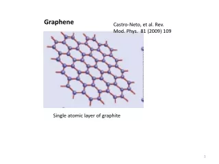
Castro-Neto, Nature Mater. 6, 176 (2007). Castro-Neto et al., Physics World (2006) Graphene: Unusual electronic structure; promising candidate for applications Microelectronics: high carrier mobility → high speed devices Resistance standard → unusual quantum Hall effect
Large scale graphene growth: Several techniques; this talk: thermal desorption of Si from SiC surface Thermal desorption of Si from SiC: large area graphene, but defects frequently observed Goal: elucidate nature of defects with the ultimate aim of reducing or eliminating the defects In particular, will focus in pseudo-six fold defect very commonly observed Properties of defect found in STM images: Near sixfold symmetry; actually threefold Sqrt(3) modulation of graphene lattice Diameter of strong modulation ~ 2 to 3 nm Center of defect is dark Dark spokes observed. Appearance of defect very similar in various experiments (Rutter et al., Science 317, 219 (2007); Guisinger et al., J. Vac. Sci. Techn A 26, 932 (2008); Simone et al., Eur. Phys. J. B 69, 351 (2009))
Energy/distance breakdown of “pinwheel” defect dI/dV plot ~ local density of states sharply peaked in energy, about 0.5 eV above the Dirac point
Methods: ab initio & tight binding Ab initio electronic structure VASP used DFT, ultrasoft pseudopotentials 212 eV plane wave cutoff 324 and 432 C-atom bilayer supercells + 1 defect 8748 k points per BZ of primitive cell STM topograph simulations Tersoff & Hamann approximation (Phys. Rev. B 31, 805 (1985)): tunneling current proportional to local density of states between Fermi level and bias V Convert constant current -> constant integrated DOS; plot height vs. position Tight binding electronic structure Mo d levels and C 2pz levels put into model Tight binding parameters determined via least squares fitting to ab initio data ~150000 k points in BZ of primitive supercell needed for converged DOS plots Up to 3888 atoms in bilayer supercell investigated
Based on pseudosixfold nature of defect and fact that it is only observed in graphene bilayers/multilayers, hypothesize that defect is on axis of the center of a hexagon in the topmost layer of Bernal stacked graphene Intercalation Substitution Adatom Defect atom can be anything: focus on Mo and Si Best fit: intercalated Mo
Graphene layers remain nearly flat (h < 0.25 A) for intercalated Mo Magnetism? Mo position Magnetic moment M(B) isolated atom 6.0 adatom 0.0 intercalated 0.0 substitution 2.0 c/w M = 2.0 for Cr substitution in monolayer (Krasheninnikov et al., PRL 102, 126807 (2009); Santos et al,arXiv:0910.0400)
324 C + 1 Mo: DOS shows three defect-associated peaks near EDirac
STM images vs. bias Tersoff and Hamann approximation: I ~ local DOS integrated from EF to E Experiment DFT simulation sqrt(3) modulation more sensitive to bias voltage than expt. central contrast dark for + bias Ebias = -0.3 eV Ebias = +0.3 eV
Can individual state(s) be identified that match experimental STM images? Plots a-g show, in order of increasing energy, the zone center states near EDirac with significant Mo d participation State E-EDirac mult. a -0.57 2 b -0.49 1 c -0.17 2 d +0.02 2 e +0.20 1 f +0.33 2 g +0.88 2 Range of E ~ 1.5 eV Bright center: singlet; m = 0; dark center; doublet; m nonzero
Simulated STM images Bilayer Trilayer Images for equivalent defect state nearly identical: Effect of intercalated Mo atom is confined to nearby layers Suggests effect of substrate is small.
Tight binding model Include only C 2pz & Mo 4d orbitals Intralayer C-C coupling to 2nd neighbors; interlayer coupling for “stacked” atoms Mo-C coupling terms to 10 neighbors shown Parameters found by least square fitting to ab initio data C-C results similar to those in literature Variance of C-C interations essential: For these terms: A = Aideal + B(d – dideal); where A, B fit to each C-C interaction parameter; guarantees correct results reproduced for ideal graphene For larger supercells, graphene distorted around Mo as in ab initio results; rest of structure “padded” with ideal graphene.
Effect of stacked (gap) vs. unstacked (gapless) C sublattices seen in ideal bilayer DOS Three strong defect peaks of ab initio calculations reproduced
Low energy peak remains nearly constant as system gets larger High energy peaks: large changes; not converged Oscillations: real or artifact of sharp distorted/undistorted boundary in model?
Energy/distance DOS: Simulation vs. Expt. Simulation Expt. Simulation; normalized +2nm 0 -2nm -1.5 1.5 -1.5 1.5 -0.2 0.8 E- EDirac (eV)
Conclusions (as of 3/31/10) Working hypothesis: experimental “pinwheel” defect is due to intercalated metal ion Biggest remaining puzzles: Why don’t fine details in STM simulations (e.g. dark spokes) agree with experiment? Why isn’t the positive energy defect peak as distinct as it seems experimentally? Most positive result: For intercalated Mo, states with energy around EDirac + 0.9 eV reproduce most results of experiments Top priorities: Extend expt. measurements to cover entire energy range of interest Extend TB model to predict STM images If necessary, vary paramters in TB model to account for possible DFT errors Most intriguing result: Simulated energy-distance plot for interstitial shows sqrt(3) modulation between sharp bounds in energy
“New” defect: rotated central region (J. Meyer, Ulm, MRS Spring meeting 2010) 6 pentagons + 6 heptagons E = +7.1 eV c/w Stone-Wales defect 2 pentagons + 2 heptagons E = + 4.2 eV Vacancy (unreconstructed) E = +10.0 eV
Conclusions (as of 4/27/10) Working hypothesis: pinwheel defect is due to rotational grain boundary type defect Biggest remaining puzzles: Why don’t fine details in STM simulations (e.g. dark spokes) agree with experiment? Why isn’t the positive energy defect peak as distinct as it seems experimentally? Most positive result: For intercalated Mo, states with energy around EDirac + 0.9 eV reproduce most results of experiments Top priorities: Extend expt. measurements to cover entire energy range of interest Extend TB model to predict STM images If necessary, vary paramters in TB model to account for possible DFT errors Most intriguing result: Simulated energy-distance plot for interstitial shows sqrt(3) modulation between sharp bounds in energy