Download
1 / 18
200 likes | 490 Views
Characterization Techniques used in the Study of Graphene. by Robert Herrick at the NanoTech User Facility. Overview. A History of the NanoTech User Facility A History of Graphene and goals for the study What is a Hall Bar? Characterization tools: Raman, AFM, Ellipsometer.

E N D
Characterization Techniques used in the Study of Graphene by Robert Herrick at the NanoTech User Facility
Overview • A History of the NanoTech User Facility • A History of Graphene and goals for the study • What is a Hall Bar? • Characterization tools: Raman, AFM, Ellipsometer
NTUF houses instruments for Nanoscale Characterization • Established in 1998 for community access to advanced lab equipment • In 2004, became 1 of 13 nodes of the NSF sponsored NNIN • National Nanotechnology Infrastructure Network • 3,000 sq ft lab in the Molecular Engineering & Sciences Building • Operates jointly with the College of Engineering's Micro Fabrication Facility • Has PhD. level trainers and lab scientists https://depts.washington.edu/ntuf/facility/index.php
Graphene a Carbon Allotrope • 2-d honeycomb lattice structure (1.4Å bond length, 3.4Å step height) • A double bond gives it high electron mobility(*3 >15kcm²/Vs @ room temp) • Strongest material ever tested 200 X as strong as steel (*4 Young’s modulus >0.5–1 TPa, Tensile strength ~130 Gpa) • Current density: 106 times that of copper, at room temperature*4 • Thermal conductivity: outperforming diamond (~5 103 W/mK, ) *4
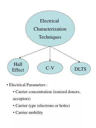
The Hall Bar • The Hall Effect • The Lorentz force • The Right Hand Rule • Can Measure the electron, hole mobility/density. 1 1 Image courtesy of http://en.wikipedia.org/wiki/Hall_effect
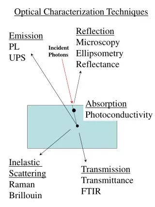
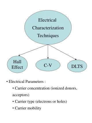
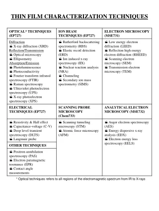
Characterization Techniques • Raman spectroscopy • Atomic force microscopy • Ellipsometry
Raman Microscopy • Raman scattered photons lose or gain energy during the scattering process • Vibrational info is specific to the chemical bonds and symmetry of molecules • Normal energy range: 200 - 4000 cm–1 • Symmetric=Raman active, Asymmetric=IR active *5 & *6
Renishaw inVia Raman Microscope • Wire 2.0 software with mapping ability • Leica DMIRBE inverted optical microscope • 10X, 50X, and 100X Objectives • Motorized X,Y,Z stage controls • Dual laser excitation sources at 514 nm and 785 nm • inVia Spectrometer • CCD camera
Atomic Force Microscopy • a form of Scanning Probe Microcopy • is limited to surface topography • in fluids or in air under ambient conditions • achieves resolutions of 10 pm • 1 nanoNewton of force per angstrom • in Dynamic/ tapping mode the feedback loop attempts to maintain a constant frequency • in Static/ contact mode the feedback loop attempts to maintain deflection of tip *2 Image from “Window on a Small World” by Nancy K. McGuire Today’s Chemist at Work June 2002
Dimension 3100 Atomic Force Microscope Hybrid XYZ Scanner: • Scan range (XY) 90 μm x 90 μm • Vertical range (Z) 7.5 μm Image resolution: • Up to 4096 points per scan line and 1024 lines Hardware: • NanoScope IVa controller • Dimension Hybrid XYZ scanner • Motorized sample stage (resolution: 2 μm) • Stage box w/ vacuum pump and illuminator • Integrated video optics • Motorized optical focus/zoom • Vibration isolation table *3 https://depts.washington.edu/ntuf/facility/docs/Dimension_Datasheet.pdf
A.F.M. RESULTS Measured step heights in the range of 10’s of nm No clean or usable Graphene measured
J.A.Woollam M2000XL Ellipsometer Specifications: Spectral range 210-1700nm Scan speed < 10 s for entire range Spot size > 1.5 mm, focused <150 µm Mapping up to 150X150 mm Automatic sample alignment Imaging via integrated CCD camera Temperature range 20 - 300 *C
Acknowledgements • North Seattle Community College • Alissa Agnello, Peter Kazarinoff • The NanoTecnology User Facility • Steven Hsieh, Arin Greenwood, Jeremiah Williams, Lindsey Maier, Paul Wallace, Xiaodong Xu, Scott Braswell and Alec Pakhomov • The University of Washington • The National Science Foundation • The National Nanotechnology Infrastructure Network
Citations *1 Steven Hsieh, Arin Greenwood, Jeremiah Williams, Lindsey Maier, Paul Wallace, Xiaodong Xu, Scott Braswell and Alec Pakhomov *2Image from “Window on a Small World” by Nancy K. McGuire Today’s Chemist at Work June 2002 *3 https://depts.washington.edu/ntuf/facility/docs/Dimension_Datasheet.pdf *4 Graphene the new Wonder Material, Mitali Kakran, Nanyang Technological University, SINGAPORE *5 http://www.doitpoms.ac.uk/tlplib/raman/raman_scattering.php *6 https://depts.washington.edu/ntuf/facility/docs/ramanschematic.pdf