Download
1 / 10
100 likes | 228 Views
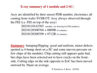
X-ray summary of 1 module and 2 SC: Assy are identified by their sensor PDB number, electronics all coming from wafer SVSB15T. Assy always observed through the FEI (i.e. FEI on top of the assy) 20210110142303 (module, see drawing for FEI numbers) 20210120300704 + 0809B (9 columns)

E N D
X-ray summary of 1 module and 2 SC: Assy are identified by their sensor PDB number, electronics all coming from wafer SVSB15T. Assy always observed through the FEI (i.e. FEI on top of the assy) 20210110142303 (module, see drawing for FEI numbers) 20210120300704 + 0809B (9 columns) 20210120300709 + 0712B (9 columns) Summary: bumping/flipping good and uniform, minor defects spotted (a 4-bump short on a SC and some uneven pressure on few chips of the module). Chip cutting still appears quite bad, but chips have been selected not to have cracks on the front-side. Cutting edge on the side opposite to EoC has been moved outward by 30mm on average. P. Netchaeva, L.Rossi 24/5/02
All chips have 9 good columns chip0 chip7 0411A 0511A 0209A 0108A 0508A 0608A 0107A 0507A HV pad 0607A 0707A 0709A 0911A 0706A 0802A 0612A 0606A chip8 chipF We look through the backside of the FEI
chip0 Chip2-3 Chip0-1 Chip1-2 Chip3-4 Chip5-6 Chip6-7 Chip4-5 chip7 X-ray of the upper part of the module (moving from left to right)
Chip0-F Chip0-1-E-F Chip1-2-D-E Chip2-3-C-D Chip3-4-B-C Chip4-5-A-B Chip5-6-9-A Chip6-7-8-9 Chip7-8 X-ray of the middle part of the module (moving from left to right)
ChipF ChipF-E ChipE-D ChipD-C ChipC-B ChipB-A ChipA-9 Chip9-8 Note: more pressure (i.e. larger bumps) on the right of each chip. Chip8 X-ray of the lower part of the module (moving from left to right)
Still the cutting edges looks bad (from the backside) with chipping going inside 100 mm or more. AMS claims that FEI chipped on the frontside have been rejected.
Spot (of In?) chip6 ChipC-D zoomed (bumps close to be shorted) ChipD-E zoomed (bumps close to be shorted) Detail of some defects
20210120300709 + 0712B short zoom zoom
The short on 20210120300709 is visible with such a magnification (quarter of chip at once), this magnification is therefore adequate to explore the chips.