Download
1 / 15
150 likes | 230 Views
Enhance D0 L1 Calorimeter Trigger for better energy measurement with modern architecture. Upgrade increases operating rate and offers improved physics selection, utilizing digital signal processing methods. Algorithm improvements reduce trigger rate and increase selectivity for high-luminosity events. The architecture includes ADF cards and custom cards for timing and synchronization. Prototype VME modules and TAB system manage data acquisition and processing efficiently.

E N D
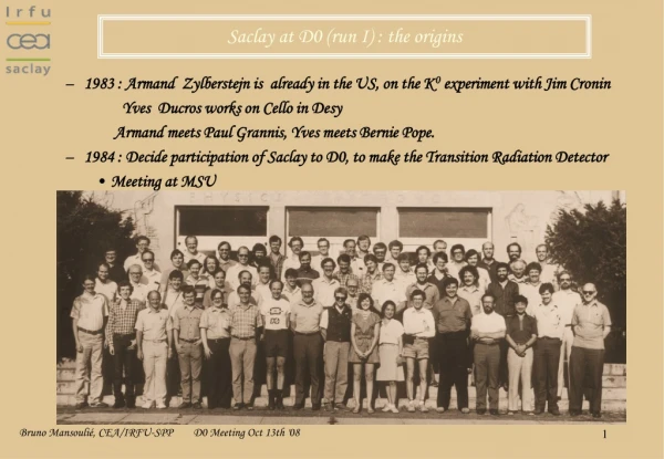
Algorithms and Architecture for the L1 Calorimeter Trigger at D0 Run IIb J. Bystricky, D. Calvet, P. Le Dû, E. Perez, G. Tarte CEA Saclay, France J. Ban, H. Evans, J. Mitrevski, J. Parsons, W. Sippach Columbia University, USA M. Abolins, D. Edmunds, P. Laurens Michigan State University, USA
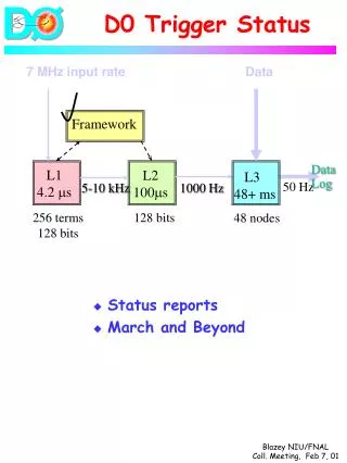
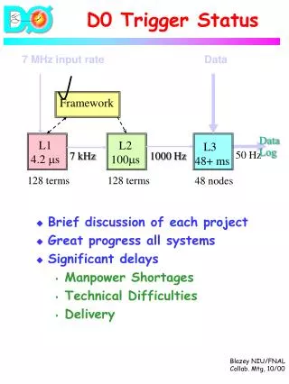
Current D0 L1 Calorimeter Trigger Cal Preamp Bunch Crossing 2.52 MHz 40 x 32 Trigger Towers 0.2 x 0.2 in Dh x Df PrecisionReadout Trigger Pickoff BLS Cardon detector Analog TT Sums 2560 differential analog Trigger pickoff signals CTFE EEt EM EM+H Compare & Sums 1280 EM samples 1280 HD samples ADC Sum / Add Trees 64 ECL bits L1 Trigger Framework L1 Yes/No ~2.6 ms after BC
Motivation for D0 L1 Calorimeter Trigger Upgrade • Improved physics selection • Current: counts of individual trigger towers above set of thresholds • Upgrade: counts of sums over sliding window greater than thresholds • Better measurement of energy in trigger towers • Current: 1 sample at peak of signal with manually set delay lines • Upgrade: optimal digital filter using up to 8 input samples • Three-fold increase of operating rate • Current: operation with 396 ns bunch spacing (2.52 MHz) • Upgrade: safe operation with 132 ns bunch spacing (7.57 MHz) • Modern and compact system • Current: 13 racks of electronics designed in 1988 • Upgrade: 3 racks of up-to date electronics
Trigger Tower Signals 396 ns 132 ns • Rise time and pulse duration not suitable for 132 ns operation: • energy seen at BC before real peak can cause pre-mature trigger • Current system: one sample at peak: sensitive to noise and jitter • Solution: Digital Signal Processing
Signal Processing Algorithm BC rate: 7.57 MHz 10 bit 30.28 MHz 10 bit 15.14 MHz 11 bit 15.14 MHz 11 bit 7.57 MHz 8 bit 7.57 MHz ADC 2 8 Tap FIR 3 Point Peak Detector 2 ET Look Up Table Analog input Serializer • Oversampling analog input at BC x 4: • short conversion latency, moderate ADC cost/power consumption • delay adjustment: programmable ADC clock inversion, selection of 2 samples to process among the 4 converted per BC • 8-tap FIR with 6 bit coefficients running at BC x 2: • improved quality results, shorter latency • 2048-entry LUT table for final calibration / clipping / saturation • 8 channels fit in 500K gate Xilinx Virtex II FPGA
Physics Selection • Longitudinal size of a jet >> Trigger Tower size (0.2 x 0.2) Current algorithm looks for jet in individual TT : Low ET QCD (background) events easily pass high ET triggers ! Need to increase selectivity for large luminosities because read-out limitations impose L1 accept rate < 5 kHz Algorithm for upgraded system • “sliding windows”sum ETof 2 x 2 TTs (RoI) • look for local maxima : compare with S2x2ET • of the 24 neighboring RoIs • trigger jetET = S4x4ET in the 4 x 4 • region around a local maxima RoI • (i.e. 0.8 x 0.8 in x ) 0.2
Single Jet reduction new current New Algorithm Sample Simulation Results new current (trigger) vs jet ET • to trigger on hard jets (ET > 40 GeV) versus inclusive trigger rate • Sharper « turn-on » curves • Reduction of trigger rate by a factor 2 to 3
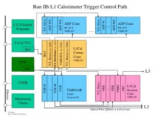
Architecture of Upgraded L1 Calorimeter Trigger • 80 ADF cards in 4 crates 6U VME64x; 8 TABs + 1 GAB in 1 crate 9U size • 2 custom cards for timing and synchronization signal fanout • Fermilab VME Interconnects + commercial PCI/VME interface in a PC for configuration and control
ADF Card • Features • 32 channels per card • analog inputs on RJ2 + fully differential AOP + zero-adjust DAC + anti-aliasing filter + 10-bit ADC + digital filter + history buffers + … • 3 digital 2 Gbit/s LVDS output links on RJ0 (32 x 8 bit x 7.57 MHz) • VME A24/D16 interface for configuration, control and monitoring • Operating modes • Calibration: self triggered data acquisition of pulse shape • System test: load then playback arbitrary data patterns • Ouptut link debug: emit constant value or pseudo-random stream • Normal operation: w/wo digital filter, w/wo peak detector, optional send raw ADC data of last L1 trigger accept, history buffer freeze for monitoring…
ADF Card Prototype VME Digital Out Analog In Channel Link Serializers VME interface & glue logic Analog Section and ADCs Core FPGA logic DC/DC converters ~1300 components on both sides of a 14-layer class 6 PCB Card in fabrication
TAB System • Features • Input from 30 ADFs (960 channels) • Sliding Windows Algorithms using serial arithmetic • Jet, EM, Tau versions • Outputs GAB Counts of clusters over threshold, ET/MET sums Cal-Trk Jet & EM clusters for matching with Tracks L2/L3 More sophisticated algorithms • Custom serial protocol for VME & Timing Interfaces • distributed by separate VME/SCL Interface board • Operating Modes • System Test: load then playback arbitrary data patterns • Normal Operation: timing/control from D0 or locally • Monitoring: data copied to registers at most steps in processing
TAB Prototype Sliding Windows Chips Channel LinkReceivers (x30) power L2/L3 Ouput (optical) VME/SCL Output to GAB ADF Inputs (x30) Output to Cal-Track (x3) card in fabrication Global Chip
ADF to TAB Links • Data duplication • Sliding window algorithm: ADF data used in 3 different TABs • TAB total cross-section = 160 Gbit/s x 3 = 480 Gbit/s • Data duplication at TAB level: challenging given bandwidth / card density • Solution: data duplicated on ADF cards by 3 identical output links • Output Links • Direct FPGA pin-to-pin LVDS connection: good coordination during design, prefer same FPGA vendor / HDL language on both ends, careful PCB layout • Solution: LVDS Channel Link chipset (National Semiconductor) • robust, simply defined and ready-to-use interface • Cabling • Solution: 240 standard cables Hard Metric 2 mm 8-pair differential
Test Hardware • Channel Link Transmitter/Receiver cards • Chipset and cable evaluation, pattern generator, test receiver,… • Active splitter card for analog trigger tower signals • connection of ADF prototype without disturbing current data taking
Summary and Future Work • Features and Benefits of upgraded D0 L1 calorimeter trigger • Improved rejection: sliding window-based physics algorithms • Better estimation of energy in calorimeter cells: digital signal processing • Compact, modern system built for operation with 132 ns bunch spacing • Architecture • 80 Analog to Digital converter and Filter cards (ADF) housed in 4 crates • 8 Trigger Algorithm Boards (TABs) and 1 Global Algorithm Board (GAB) • 2 custom modules for synchronization, 5 VME interface pairs, 2 PCI/VME interface and 1 PC for configuration and control • Implementation • Prototypes of ADF and TAB cards under assembly • Production and installation of full system at D0 for operation in 2006